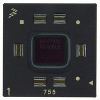
MPC755CRX400LE Freescale Semiconductor, MPC755CRX400LE Datasheet - Page 17

MPC755CRX400LE
Manufacturer Part Number
MPC755CRX400LE
Description
IC MPU 32BIT 400MHZ PPC 360-CBGA
Manufacturer
Freescale Semiconductor
Datasheet
1.MPC755BPX300LE.pdf
(56 pages)
Specifications of MPC755CRX400LE
Processor Type
MPC7xx PowerPC 32-Bit
Speed
400MHz
Voltage
2V
Mounting Type
Surface Mount
Package / Case
360-FCCBGA
Family Name
MPC7xx
Device Core
PowerPC
Device Core Size
64b
Frequency (max)
400MHz
Instruction Set Architecture
RISC
Supply Voltage 1 (typ)
2V
Operating Supply Voltage (max)
2.1V
Operating Supply Voltage (min)
1.9V
Operating Temp Range
0C to 105C
Operating Temperature Classification
Commercial
Mounting
Surface Mount
Pin Count
360
Package Type
FCCBGA
Lead Free Status / RoHS Status
Contains lead / RoHS non-compliant
Features
-
Lead Free Status / Rohs Status
Not Compliant
Available stocks
Company
Part Number
Manufacturer
Quantity
Price
Company:
Part Number:
MPC755CRX400LE
Manufacturer:
MOT
Quantity:
12 388
Company:
Part Number:
MPC755CRX400LE
Manufacturer:
Freescale Semiconductor
Quantity:
10 000
Electrical and Thermal Characteristics
SRAM. Note that revisions of the MPC755 prior to Rev. 2.8 (Rev. E) were limited in performance, and
were typically limited to 175 MHz with similarly-rated SRAM. For more information, see
Section 10.2,
“Part Numbers Not Fully Addressed by This Document.”
Freescale is similarly limited by system constraints and cannot perform tests of the L2 interface on a
socketed part on a functional tester at the maximum frequencies of
Table
11. Therefore, functional
operation and AC timing information are tested at core-to-L2 divisors of 2 or greater. Functionality of
core-to-L2 divisors of 1 or 1.5 is verified at less than maximum rated frequencies.
L2 input and output signals are latched or enabled, respectively, by the internal L2CLK (which is SYSCLK
multiplied up to the core frequency and divided down to the L2CLK frequency). In other words, the AC
timings of
Table 12
and
Table 13
are entirely independent of L2SYNC_IN. In a closed loop system, where
L2SYNC_IN is driven through the board trace by L2SYNC_OUT, L2SYNC_IN only controls the output
phase of L2CLK_OUTA and L2CLK_OUTB which are used to latch or enable data at the SRAMs.
However, since in a closed loop system L2SYNC_IN is held in phase alignment with the internal L2CLK,
the signals of
Table 12
and
Table 13
are referenced to this signal rather than the not-externally-visible
internal L2CLK. During manufacturing test, these times are actually measured relative to SYSCLK.
The L2SYNC_OUT signal is intended to be routed halfway out to the SRAMs and then returned to the
L2SYNC_IN input of the MPC755 to synchronize L2CLK_OUT at the SRAM with the processor’s
internal clock. L2CLK_OUT at the SRAM can be offset forward or backward in time by shortening or
lengthening the routing of L2SYNC_OUT to L2SYNC_IN. See Freescale Application Note AN1794/D,
Backside L2 Timing Analysis for PCB Design Engineers.
The L2CLK_OUTA and L2CLK_OUTB signals should not have more than two loads.
MPC755 RISC Microprocessor Hardware Specifications, Rev. 8
Freescale Semiconductor
17


