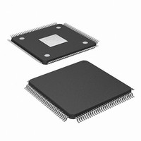
XS1-L01A-TQ128-C4-THS XMOS, XS1-L01A-TQ128-C4-THS Datasheet - Page 8

XS1-L01A-TQ128-C4-THS
Manufacturer Part Number
XS1-L01A-TQ128-C4-THS
Description
IC MPU 32BIT SINGLE CORE 128TQFP
Manufacturer
XMOS
Datasheet
1.XS1-L01A-TQ128-C5.pdf
(26 pages)
Specifications of XS1-L01A-TQ128-C4-THS
Processor Type
XCore 32-Bit
Speed
400MHz
Voltage
0.95 V ~ 1.05 V
Mounting Type
Surface Mount
Package / Case
128-TQFP Exposed Pad, 128-eTQFP, 128-HTQFP, 128-VQFP
Lead Free Status / RoHS Status
Lead free / RoHS Compliant
Features
-
Other names
880-1023
Available stocks
Company
Part Number
Manufacturer
Quantity
Price
XS1-L1 128TQFP Datasheet (2.2)
These signals control the on-chip PLL of the XS1-L1
3 System Services
System Services are required to support correct device behavior. These signals
control clocking, reset and boot behavior of the device.
3.1 Clock control signals
Functional description
PLL_AVDD The PLL requires a very clean AVDD power supply. It is recommended
PLL_AGND Analog ground for the PLL. Connect directly to board ground.
CLK Reference clock input for the PLL. This signal is used as a reference by the PLL
3.2 Miscellaneous control signals
Functional description
MODE[3:0] These pins determine the boot source and PLL boot mode of the device.
Signal
PLL_AVDD
PLL_AGND
CLK
Signal
MODE[3:0]
DEBUG
RST_N
that this supply node be separated from the other, noisier, supplies on the
board. The supply should be decoupled close to the respective IC package pin.
Nominally 1.0V.
in generating all on chip clocks.
Bits [3:2] control the boot source according to the following table:
Pin ID
48
47
25
Pin ID
55, 53, 52, 51
42
21
I/O
pwr
pwr
I, PD, ST
I/O
I, PU, ST
IO, PU
I, PU, ST
Description
Analog power supply for the PLL
Analog ground for the PLL
Reference clock input for the PLL
Description
Sets boot mode
Multi-device debug
Asynchronous system reset
8/26


