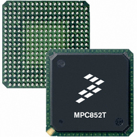
MPC852TVR100A Freescale Semiconductor, MPC852TVR100A Datasheet - Page 15

MPC852TVR100A
Manufacturer Part Number
MPC852TVR100A
Description
IC MPU POWERQUICC 100MHZ 256PBGA
Manufacturer
Freescale Semiconductor
Series
PowerQUICC Ir
Datasheet
1.MPC852TVR50A.pdf
(80 pages)
Specifications of MPC852TVR100A
Processor Type
MPC8xx PowerQUICC 32-Bit
Speed
100MHz
Voltage
1.8V
Mounting Type
Surface Mount
Package / Case
256-PBGA
Processor Series
MPC8xx
Core
MPC8xx
Data Bus Width
32 bit
Development Tools By Supplier
MPC852TADS-KIT
Maximum Clock Frequency
100 MHz
Operating Supply Voltage
0 V to 3.3 V
Maximum Operating Temperature
+ 105 C
Mounting Style
SMD/SMT
Data Ram Size
8 KB
I/o Voltage
3.3 V
Interface Type
SPI, UART
Minimum Operating Temperature
0 C
Program Memory Size
4 KB
Program Memory Type
EPROM/Flash
Core Size
32 Bit
Cpu Speed
100MHz
Embedded Interface Type
SPI, UART
Digital Ic Case Style
BGA
No. Of Pins
256
Supply Voltage Range
1.7V To 1.9V
Rohs Compliant
Yes
Lead Free Status / RoHS Status
Contains lead / RoHS non-compliant
Features
-
Lead Free Status / Rohs Status
Lead free / RoHS Compliant
Available stocks
Company
Part Number
Manufacturer
Quantity
Price
Company:
Part Number:
MPC852TVR100A
Manufacturer:
MOTOROLA
Quantity:
490
Company:
Part Number:
MPC852TVR100A
Manufacturer:
Freescale Semiconductor
Quantity:
10 000
Freescale Semiconductor
B11a
B12a
B13a
Num
B7a
B7b
B8a
B8b
B11
B12
B13
B14
B3
B4
B5
B7
B8
B9
CLKOUT pulse width high (MIN = 0.4 × B1,
MAX = 0.6 × B1)
CLKOUT rise time
CLKOUT fall time
CLKOUT to A(0:31), BADDR(28:30),
RD/WR, BURST, D(0:31), DP(0:3) output
hold (MIN = 0.25 × B1)
CLKOUT to TSIZ(0:1), REG, RSV, BDIP ,
PTR output hold (MIN = 0.25 × B1)
CLKOUT to BR, BG, FRZ, VFLS(0:1),
VF(0:2) IWP(0:2), LWP(0:1), STS output
hold (MIN = 0.25 × B1)
CLKOUT to A(0:31), BADDR(28:30)
RD/WR, BURST, D(0:31), DP(0:3) valid
(MAX = 0.25 × B1 + 6.3)
CLKOUT to TSIZ(0:1), REG, RSV, BDIP ,
PTR valid (MAX = 0.25 × B1 + 6.3)
CLKOUT to BR, BG, VFLS(0:1), VF(0:2),
IWP(0:2), FRZ, LWP(0:1), STS Valid
(MAX = 0.25 × B1 + 6.3)
CLKOUT to A(0:31), BADDR(28:30),
RD/WR, BURST, D(0:31), DP(0:3),
TSIZ(0:1), REG, RSV, PTR High-Z
(MAX = 0.25 × B1 + 6.3)
CLKOUT to TS, BB assertion
(MAX = 0.25 × B1 + 6.0)
CLKOUT to TA, BI assertion (when driven
by the memory controller or PCMCIA
interface) (MAX = 0.00 × B1 + 9.30
CLKOUT to TS, BB negation
(MAX = 0.25 × B1 + 4.8)
CLKOUT to TA, BI negation (when driven
by the memory controller or PCMCIA
interface) (MAX = 0.00 × B1 + 9.00)
CLKOUT to TS, BB High-Z
(MIN = 0.25 × B1)
CLKOUT to TA, BI High-Z (when driven by
the memory controller or PCMCIA
interface) (MIN = 0.00 × B1 + 2.5)
CLKOUT to TEA assertion
(MAX = 0.00 × B1 + 9.00)
Characteristic
MPC852T PowerQUICC™ Hardware Specifications, Rev. 4
Table 9. Bus Operation Timings (continued)
2
)
3
12.1
7.60
7.60
7.60
7.60
7.60
2.50
7.60
2.50
7.60
2.50
2.50
Min
—
—
—
—
—
33 MHz
13.80
13.80
13.80
13.80
13.60
12.30
21.60
15.00
Max
18.2
4.00
4.00
9.30
9.00
9.00
—
—
—
10.0
6.30
6.30
6.30
6.30
6.30
2.50
6.30
2.50
6.30
2.50
2.50
Min
—
—
—
—
—
40 MHz
12.50
12.50
12.50
12.50
12.30
11.00
20.30
15.00
Max
15.0
4.00
4.00
9.30
9.00
9.00
—
—
—
5.00
5.00
5.00
5.00
5.00
2.50
5.00
2.50
5.00
2.50
2.50
Min
8.0
—
—
—
—
—
50 MHz
11.30
11.30
11.30
11.30
11.00
19.00
15.00
Max
12.0
4.00
4.00
9.30
9.80
9.00
9.00
—
—
—
3.80
3.80
3.80
3.80
3.80
2.50
3.80
3.80
2.50
2.50
2.50
Min
6.1
—
—
—
—
—
66 MHz
Bus Signal Timing
10.00
10.00
10.00
10.00
14.00
15.00
Max
4.00
4.00
9.80
9.80
8.50
9.00
9.00
9.1
—
—
—
Unit
ns
ns
ns
ns
ns
ns
ns
ns
ns
ns
ns
ns
ns
ns
ns
ns
ns
15


