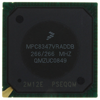
MPC8347VRADDB Freescale Semiconductor, MPC8347VRADDB Datasheet - Page 19

MPC8347VRADDB
Manufacturer Part Number
MPC8347VRADDB
Description
IC MPU POWERQUICC II 620-PBGA
Manufacturer
Freescale Semiconductor
Series
PowerQUICC II PROr
Specifications of MPC8347VRADDB
Processor Type
MPC83xx PowerQUICC II Pro 32-Bit
Speed
266MHz
Voltage
1.2V
Mounting Type
Surface Mount
Package / Case
620-PBGA
Processor Series
MPC8xxx
Core
e300
Data Bus Width
32 bit
Development Tools By Supplier
MPC8349E-MITXE
Maximum Clock Frequency
266 MHz
Maximum Operating Temperature
+ 105 C
Mounting Style
SMD/SMT
I/o Voltage
1.8 V, 2.5 V, 3.3 V
Minimum Operating Temperature
0 C
Core Size
32 Bit
Program Memory Size
64KB
Cpu Speed
266MHz
Embedded Interface Type
I2C, SPI, USB, UART
Digital Ic Case Style
BGA
No. Of Pins
672
Rohs Compliant
Yes
Lead Free Status / RoHS Status
Lead free / RoHS Compliant
Features
-
Lead Free Status / Rohs Status
Lead free / RoHS Compliant
Available stocks
Company
Part Number
Manufacturer
Quantity
Price
Company:
Part Number:
MPC8347VRADDB
Manufacturer:
Freescale Semiconductor
Quantity:
135
Company:
Part Number:
MPC8347VRADDB
Manufacturer:
Freescale Semiconductor
Quantity:
10 000
Table 15
Figure 7
Table 16
signals of the DDR controller for various loadings, which can be useful for a system utilizing the DLL.
These numbers are the result of simulations for one topology. The delay numbers will strongly depend on
the topology used. These delay numbers show the total delay for the address and command to arrive at the
DRAM devices. The actual delay could be different than the delays seen in simulation, depending on the
system topology. If a heavily loaded system is used, the DLL loop may need to be adjusted to meet setup
requirements at the DRAM.
Freescale Semiconductor
V
V
Notes:
1. Data input threshold measurement point.
2. Data output measurement point.
OUT
TH
ADDR/CMD
MDQS[n]
shows the DDR SDRAM output timing diagram for source synchronous mode.
shows the DDR SDRAM measurement conditions.
provides approximate delay information that can be expected for the address and command
MDQ[x]
MCK[n]
MCK[n]
MPC8347E PowerQUICC™ II Pro Integrated Host Processor Hardware Specifications, Rev. 11
Figure 7. DDR SDRAM Output Timing Diagram for Source Synchronous Mode
Output
Table 15. DDR SDRAM Measurement Conditions
Write A0
Symbol
t
DDKHAS
t
DDKHDX
Figure 6. DDR AC Test Load
t
MCK
Z
0
,t
= 50 Ω
t
DDKHCS
DDKHAX
NOOP
D0
, t
t
DDKHCX
DDKHDS
t
t
DDKHMP
DDKHMH
D1
t
DDKLDS
R
t
DDKLDX
L
= 50 Ω
MV
0.5 × GV
REF
DDR
OV
± 0.31 V
DD
DD
/2
t
DDKHME
Unit
V
V
DDR SDRAM
Notes
1
2
19


