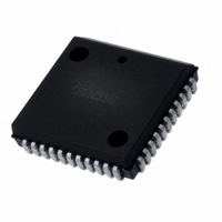
CS80C286-12 Intersil, CS80C286-12 Datasheet - Page 30

CS80C286-12
Manufacturer Part Number
CS80C286-12
Description
IC CPU 16BIT 5V 12.5MHZ 68-PLCC
Manufacturer
Intersil
Datasheet
1.CS80C286-12.pdf
(60 pages)
Specifications of CS80C286-12
Processor Type
80C286 16-Bit
Speed
12.5MHz
Voltage
5V
Mounting Type
Surface Mount
Package / Case
68-PLCC
Lead Free Status / RoHS Status
Contains lead / RoHS non-compliant
Features
-
Available stocks
Company
Part Number
Manufacturer
Quantity
Price
Company:
Part Number:
CS80C286-12
Manufacturer:
INTERSIL
Quantity:
5 510
Part Number:
CS80C286-12
Manufacturer:
HAR
Quantity:
20 000
Bus Cycle Termination
At maximum transfer rates, the 80C286 bus alternates
between the status and command states. The bus status
signals become inactive after T
signal the start of the next bus operation after the completion
of the current cycle. No external indication of T
the 80C286 local bus. The bus master and bus controller
enter T
until terminated by the assertion of READY.
READY Operation
The current bus master and 82C288 bus controller terminate
each bus operation simultaneously to achieve maximum bus
operation bandwidth. Both are informed in advance by
READY active (open-collector output from 82C284) which
identifies the last T
bus master and bus controller must see the same sense of
the READY signal, thereby requiring READY to be synchro-
nous to the system clock.
Synchronous Ready
The 82C284 clock generator provides READY synchroniza-
tion from both synchronous and asynchronous sources (see
Figure 24). The synchronous ready input (SRDY) of the
clock generator is sampled with the falling edge of CLK at
EX1
EX2
C
A
S1 • S0
READY
CMDLY
CMDLY
23
PROC
directly after T
CLK
CLK
ALE
- A
RD
RD
0
φ1
C
VALID ADDR (N-1)
cycle of the current bus operation. The
S
T
FIGURE 23. CMDLY CONTROLS THE LEADING EDGE OF COMMAND SIGNAL
S
and continue executing T
φ2
S
so that they may correctly
READ CYCLE N -1
φ1
T
C
φ2
C
exists on
C
cycles
80C286
φ1
30
the end of phase 1 of each T
broadcast to the bus master and bus controller via the
READY output line.
Asynchronous Ready
Many systems have devices or subsystems that are asyn-
chronous to the system clock. As a result, their ready out-
puts cannot be guaranteed to meet the 82C284 SRDY setup
and hold time requirements. But the 82C284 asynchronous
ready input (ARDY) is designed to accept such signals. The
ARDY input is sampled at the beginning of each T
82C284 synchronization logic. This provides one system
CLK cycle time to resolve its value before broadcasting it to
the bus master and bus controller.
ARDY or ARDYEN must be HIGH at the end of T
cannot be used to terminate the bus cycle with no wait
states.
Each ready input of the 82C284 has an enable pin
(SRDYEN and ARDYEN) to select whether the current bus
operation will be terminated by the synchronous or asyn-
chronous ready. Either of the ready inputs may terminate a
bus operation. These enable inputs are active low and have
the same timing as their respective ready inputs. Address
decode logic usually selects whether the current bus opera-
tion should be terminated by ARDY or SRDY.
T
C
VALID ADDR N
φ2
φ1
T
S
φ2
READ CYCLE N
C
. The state of SRDY is then
φ1
T
C
φ2
C
S
cycle by
. ARDY


