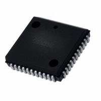
CS80C286-12 Intersil, CS80C286-12 Datasheet - Page 51

CS80C286-12
Manufacturer Part Number
CS80C286-12
Description
IC CPU 16BIT 5V 12.5MHZ 68-PLCC
Manufacturer
Intersil
Datasheet
1.CS80C286-12.pdf
(60 pages)
Specifications of CS80C286-12
Processor Type
80C286 16-Bit
Speed
12.5MHz
Voltage
5V
Mounting Type
Surface Mount
Package / Case
68-PLCC
Lead Free Status / RoHS Status
Contains lead / RoHS non-compliant
Features
-
Available stocks
Company
Part Number
Manufacturer
Quantity
Price
Company:
Part Number:
CS80C286-12
Manufacturer:
INTERSIL
Quantity:
5 510
Part Number:
CS80C286-12
Manufacturer:
HAR
Quantity:
20 000
Waveforms
80C286 Instruction Set Summary
Instruction Timing Notes
The instruction clock counts listed below establish the maxi-
mum execution rate of the 80C286. With no delays in bus
cycles, the actual clock count of an 80C286 program will
average 5% more than the calculated clock count, due to
instruction sequences which execute faster than they can be
fetched from memory.
To calculate elapsed times for instruction sequences, multi-
ply the sum of all instruction clock counts, as listed in the
table below, by the processor clock period. An 12.5MHz pro-
cessor clock has a clock period of 80 nanoseconds and
requires an 80C286 system clock (CLK input) of 25MHz.
Instruction Clock Count Assumptions
Instruction Set Summary Notes
Addressing displacements selected by the MOD field are not
shown. If necessary they appear after the instruction fields
shown.
1. The instruction has been perfected, decoded and is
2. Bus cycles do not require wait states.
3. There are no processor extension data transfer or local
4. No exceptions occur during instruction execution.
7 6 5 4 3 2 1 0 7 6 5 4 3 2 1 0
7 6 5 4 3 2 1 0 7 6 5 4 3 2 1 0 7 6 5 4 3 2 1 0
ready for execution. Control transfer instruction clock
counts include all time required to fetch, decode, and
prepare the next instruction for execution.
bus HOLD requests.
OPCODE
BYTE 1
BYTE 1
LONG OPCODE
d w
(Continued)
MOD
REG
BYTE 2
BYTE 2
FIGURE 40. 80C286 INSTRUCTION FORMAT EXAMPLES
R/M
FIGURE 40A. SHORT OPCODE FORMAT EXAMPLE
FIGURE 40B. LONG OPCODE FORMAT EXAMPLE
REGISTER OPERAND REGISTERS TO USE IN OFFSET CALCULATION
REGISTER OPERAND/EXTENSION OF OPCODE
REGISTER MODE/MEMORY MODE WITH DISPLACEMENT LENGTH
WORD/BYTE OPERATION
DIRECTION IS TO REGISTER DIRECTION IS FROM REGISTER
OPERATION (INSTRUCTION) CODE
MOD
LOW DISP/DATA
BYTE 3
REG
BYTE 3
80C286
R/M
51
Above/below refers to unsigned value.
Greater refers to more positive signed values.
Less refers to less positive (more negative) signed values
if d = 1, then “to” register; if d = 0 then “from” register
if w = 1, then word instruction; if w = 0, then byte instruction
if s = 0, then 16-bit immediate data form the operand
if s = 1, then an immediate data byte is sign-extended to
form the 16-bit operand
x don’t care
z used for string primitives for comparison with ZF FLAG
If two clock counts are given, the smaller refers to a register
operand and the larger refers to a memory operand
* = add one clock if offset calculation requires summing 3
n = number of times repeated
m = number of bytes of code in next instruction
Level (L) - Lexical nesting level of the procedure
The following comments describe possible exceptions, side
effects and allowed usage for instructions in both operating
modes of the 80C286.
HIGH DISP/DATA
LOW DISP
elements
BYTE 4
BYTE 4
LOW DATA
HIGH DISP
BYTE 5
BYTE 5
HIGH DATA
BYTE 6


