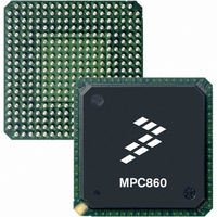
MPC855TZQ80D4 Freescale Semiconductor, MPC855TZQ80D4 Datasheet - Page 52

MPC855TZQ80D4
Manufacturer Part Number
MPC855TZQ80D4
Description
IC MPU POWERQUICC 80MHZ 357PBGA
Manufacturer
Freescale Semiconductor
Series
PowerQUICCr
Specifications of MPC855TZQ80D4
Processor Type
MPC8xx PowerQUICC 32-Bit
Speed
80MHz
Voltage
3.3V
Mounting Type
Surface Mount
Package / Case
357-PBGA
Processor Series
MPC8xx
Core
MPC8xx
Data Bus Width
32 bit
Maximum Clock Frequency
80 MHz
Operating Supply Voltage
2.5 V, 3.3 V
Maximum Operating Temperature
+ 95 C
Mounting Style
SMD/SMT
Minimum Operating Temperature
0 C
Core Size
32 Bit
Program Memory Size
8KB
Cpu Speed
80MHz
Digital Ic Case Style
BGA
No. Of Pins
357
Supply Voltage Range
3.135V To 3.465V
Rohs Compliant
No
Features
-
Lead Free Status / Rohs Status
Lead free / RoHS Compliant
Available stocks
Company
Part Number
Manufacturer
Quantity
Price
Company:
Part Number:
MPC855TZQ80D4
Manufacturer:
Freescale Semiconductor
Quantity:
10 000
Part Number:
MPC855TZQ80D4
Manufacturer:
FREESCALE
Quantity:
20 000
I2C
Figure 36
12 I
This section describes the DC and AC electrical characteristics for the I
12.1
Table 39
52
At recommended operating conditions with OV
Input high voltage level
Input low voltage level
Low level output voltage
Output fall time from V
capacitance from 10 to 400 pF
Pulse width of spikes which must be suppressed by the
input filter
Input current each I/O pin (input voltage is between 0.1 ×
OV
Capacitance for each I/O pin
Notes:
1. Output voltage (open drain or open collector) condition = 3 mA sink current.
2. C
3. Refer to the MPC8555E PowerQUICC™ III Integrated Communications Processor Reference Manual for information on the
4. I/O pins obstruct the SDA and SCL lines if OV
digital filter used.
DD
B
= capacitance of one bus line in pF.
and 0.9 × OV
MPC8555E PowerQUICC™ III Integrated Communications Processor Hardware Specification, Rev. 4.2
2
provides the DC electrical characteristics for the I
I
C
provides the test access port timing diagram.
External Clock
2
C DC Electrical Characteristics
TDI, TMS
DD
JTAG
TDO
TDO
(max)
IH
Parameter
(min) to V
t
Output Data Valid
JTKLOX
IL
(max) with a bus
Figure 36. Test Access Port Timing Diagram
Table 39. I
DD
of 3.3 V ± 5%.
t
VM
JTKLOZ
VM = Midpoint Voltage (OV DD /2)
t
JTKLOV
DD
2
C DC Electrical Characteristics
is switched off.
Symbol
t
t
I2KLKV
I2KHKL
V
V
V
C
OL
I
IH
IL
t
I
I
JTIVKH
2
C interface of the MPC8555E.
20 + 0.1 × C
0.7 × OV
Output Data Valid
–0.3
Min
–10
Data Valid
—
0
0
Input
VM
DD
B
2
C interface of the MPC8555E.
0.3 × OV
0.2 × OV
OV
Max
DD
250
t
50
10
10
JTIXKH
+ 0.3
DD
DD
Freescale Semiconductor
Unit
μA
pF
ns
ns
V
V
V
Notes
1
2
3
4


