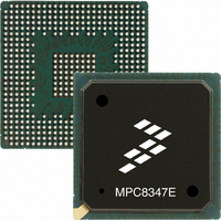
MPC8347EVVALFB Freescale Semiconductor, MPC8347EVVALFB Datasheet - Page 43

MPC8347EVVALFB
Manufacturer Part Number
MPC8347EVVALFB
Description
IC MPU POWERQUICC II 672-TBGA
Manufacturer
Freescale Semiconductor
Series
PowerQUICC II PROr
Specifications of MPC8347EVVALFB
Processor Type
MPC83xx PowerQUICC II Pro 32-Bit
Speed
667MHz
Voltage
1.3V
Mounting Type
Surface Mount
Package / Case
672-TBGA
Processor Series
MPC8xxx
Core
e300
Data Bus Width
32 bit
Development Tools By Supplier
MPC8349E-MITXE
Maximum Clock Frequency
667 MHz
Maximum Operating Temperature
+ 105 C
Mounting Style
SMD/SMT
I/o Voltage
1.8 V, 2.5 V, 3.3 V
Minimum Operating Temperature
0 C
Core Size
32 Bit
Program Memory Size
64KB
Cpu Speed
667MHz
Embedded Interface Type
I2C, SPI, USB, UART
Digital Ic Case Style
TBGA
No. Of Pins
672
Rohs Compliant
Yes
Family Name
MPC83xx
Device Core
PowerQUICC II Pro
Device Core Size
32b
Frequency (max)
667MHz
Instruction Set Architecture
RISC
Supply Voltage 1 (typ)
1.3V
Operating Supply Voltage (max)
1.36V
Operating Supply Voltage (min)
1.24V
Operating Temp Range
0C to 105C
Operating Temperature Classification
Commercial
Mounting
Surface Mount
Pin Count
672
Package Type
TBGA
Lead Free Status / RoHS Status
Lead free / RoHS Compliant
Features
-
Lead Free Status / Rohs Status
Lead free / RoHS Compliant
Available stocks
Company
Part Number
Manufacturer
Quantity
Price
Company:
Part Number:
MPC8347EVVALFB
Manufacturer:
Freescale Semiconductor
Quantity:
135
Company:
Part Number:
MPC8347EVVALFB
Manufacturer:
Freescale Semiconductor
Quantity:
10 000
Part Number:
MPC8347EVVALFB
Manufacturer:
FREESCALE
Quantity:
20 000
Figure 26
Figure 27
Freescale Semiconductor
At recommended operating conditions (see
Output hold times:
Notes:
1. All outputs are measured from the midpoint voltage of the falling/rising edge of t
2. The symbols for timing specifications follow the pattern of t
4. Non-JTAG signal input timing with respect to t
5. Non-JTAG signal output timing with respect to t
6. Guaranteed by design and characterization.
JTAG external clock to output high impedance:
3. TRST is an asynchronous level sensitive signal. The setup time is for test purposes only.
Time-of-flight delays must be added for trace lengths, vias, and connectors in the system.
and t
(JT) with respect to the time data input signals (D) reaching the valid state (V) relative to the t
The output timings are measured at the pins. All output timings assume a purely resistive 50 Ω load (see
to the high (H) state or setup time. Also, t
went invalid (X) relative to the t
based on three letters representing the clock of a particular function. For rise and fall times, the latter convention is used with
the appropriate letter: R (rise) or F (fall).
(first two letters of functional block)(reference)(state)(signal)(state)
provides the AC test load for TDO and the boundary-scan outputs of the MPC8347E.
provides the JTAG clock input timing diagram.
MPC8347E PowerQUICC™ II Pro Integrated Host Processor Hardware Specifications, Rev. 11
External Clock
Table 37. JTAG AC Timing Specifications (Independent of CLKIN)
Parameter
JTAG
Output
JTG
Figure 26. AC Test Load for the JTAG Interface
Figure 27. JTAG Clock Input Timing Diagram
Boundary-scan data
Boundary-scan data
clock reference (K) going to the high (H) state. In general, the clock reference symbol is
Table
VM
t
JTKHKL
JTDXKH
2).
VM = Midpoint Voltage (OV DD /2)
TCLK
Z
t
JTG
TCLK
0
symbolizes JTAG timing (JT) with respect to the time data input signals (D)
= 50 Ω
TDO
TDO
.
VM
.
for outputs. For example, t
(first two letters of functional block)(signal)(state)(reference)(state)
Symbol
t
t
t
t
JTKLDX
JTKLOX
JTKLOZ
JTKLDZ
VM
2
R
L
= 50 Ω
Min
TCLK
t
2
2
2
2
JTGR
to the midpoint of the signal in question.
JTDVKH
OV
DD
1
Max
symbolizes JTAG device timing
19
—
—
t
9
(continued)
JTG
JTGF
/2
clock reference (K) going
Unit
ns
ns
Figure
for inputs
26).
Notes
5, 6
5
JTAG
43


