MPC8321CZQADDC Freescale Semiconductor, MPC8321CZQADDC Datasheet - Page 29
MPC8321CZQADDC
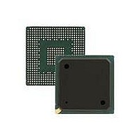
Manufacturer Part Number
MPC8321CZQADDC
Description
IC MPU PWRQUICC II 516-PBGA
Manufacturer
Freescale Semiconductor
Datasheet
1.MPC8321VRADDC.pdf
(82 pages)
Specifications of MPC8321CZQADDC
Processor Type
MPC83xx PowerQUICC II Pro 32-Bit
Speed
266MHz
Voltage
1V
Mounting Type
Surface Mount
Package / Case
516-PBGA
Processor Series
MPC8xxx
Core
e300
Data Bus Width
32 bit
Development Tools By Supplier
MPC8323E-MDS-PB
Maximum Clock Frequency
266 MHz
Maximum Operating Temperature
+ 105 C
Mounting Style
SMD/SMT
Data Ram Size
16 KB
I/o Voltage
1.8 V, 3.3 V
Interface Type
I2C, SPI, UART
Minimum Operating Temperature
- 40 C
Family Name
MPC83xx
Device Core
PowerQUICC II Pro
Device Core Size
32b
Frequency (max)
266MHz
Instruction Set Architecture
RISC
Supply Voltage 1 (typ)
1V
Operating Supply Voltage (max)
1.05V
Operating Supply Voltage (min)
0.95V
Operating Temp Range
-40C to 105C
Operating Temperature Classification
Industrial
Mounting
Surface Mount
Pin Count
516
Package Type
TEBGA
Lead Free Status / RoHS Status
Lead free / RoHS Compliant
Features
-
Lead Free Status / Rohs Status
Lead free / RoHS Compliant
Available stocks
Company
Part Number
Manufacturer
Quantity
Price
Company:

Part Number:
MPC8321CZQADDC
Manufacturer:
MOTOROLA
Quantity:
996
Company:
Part Number:
MPC8321CZQADDC
Manufacturer:
Freescale Semiconductor
Quantity:
10 000


10 JTAG
This section describes the DC and AC electrical specifications for the IEEE Std. 1149.1™ (JTAG)
interface of the MPC8323E.
10.1
Table 31
MPC8323E.
Freescale Semiconductor
Output high voltage
Output low voltage
Output low voltage
Input high voltage
MPC8323E PowerQUICC II Pro Integrated Communications Processor Family Hardware Specifications, Rev. 4
GPCM Mode Output Signals:
LCS[0:3]/LBS[0:1]/LGPL[0:5]
UPM Mode Output Signals:
provides the DC electrical characteristics for the IEEE Std. 1149.1 (JTAG) interface of the
JTAG DC Electrical Characteristics
UPM Mode Input Signal:
Characteristic
Figure 17. Local Bus Signals, GPCM/UPM Signals for LCRR[CLKDIV] = 4
LCS[0:3]/LWE
Input Signals:
LUPWAIT
LAD[0:15]
Table 31. JTAG Interface DC Electrical Characteristics
LCLK
T1
T2
T3
T4
t
t
LBKHOV
LBKHOV
Symbol
V
V
V
V
OH
OL
OL
IH
t
LBIVKH
I
OH
I
t
t
I
OL
LBKHOZ
LBKHOZ
OL
Condition
= –6.0 mA
= 3.2 mA
= 6.0 mA
—
t
LBIVKH
t
LBIXKH
Min
2.4
2.5
—
—
OV
DD
Max
0.5
0.4
—
t
LBIXKH
+ 0.3
Unit
V
V
V
V
JTAG
29
Related parts for MPC8321CZQADDC
Image
Part Number
Description
Manufacturer
Datasheet
Request
R

Part Number:
Description:
Manufacturer:
Freescale Semiconductor, Inc
Datasheet:
Part Number:
Description:
Manufacturer:
Freescale Semiconductor, Inc
Datasheet:
Part Number:
Description:
Manufacturer:
Freescale Semiconductor, Inc
Datasheet:
Part Number:
Description:
Manufacturer:
Freescale Semiconductor, Inc
Datasheet:
Part Number:
Description:
Manufacturer:
Freescale Semiconductor, Inc
Datasheet:
Part Number:
Description:
Manufacturer:
Freescale Semiconductor, Inc
Datasheet:
Part Number:
Description:
Manufacturer:
Freescale Semiconductor, Inc
Datasheet:
Part Number:
Description:
Manufacturer:
Freescale Semiconductor, Inc
Datasheet:
Part Number:
Description:
Manufacturer:
Freescale Semiconductor, Inc
Datasheet:
Part Number:
Description:
Manufacturer:
Freescale Semiconductor, Inc
Datasheet:
Part Number:
Description:
Manufacturer:
Freescale Semiconductor, Inc
Datasheet:
Part Number:
Description:
Manufacturer:
Freescale Semiconductor, Inc
Datasheet:
Part Number:
Description:
Manufacturer:
Freescale Semiconductor, Inc
Datasheet:
Part Number:
Description:
Manufacturer:
Freescale Semiconductor, Inc
Datasheet:
Part Number:
Description:
Manufacturer:
Freescale Semiconductor, Inc
Datasheet: