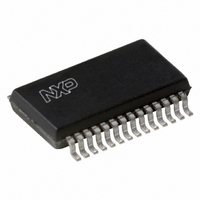
UDA1342TS/N1,518 NXP Semiconductors, UDA1342TS/N1,518 Datasheet - Page 14

UDA1342TS/N1,518
Manufacturer Part Number
UDA1342TS/N1,518
Description
IC AUDIO CODEC 24BIT 28SSOP
Manufacturer
NXP Semiconductors
Type
Stereo Audior
Datasheet
1.UDA1342TSN1518.pdf
(45 pages)
Specifications of UDA1342TS/N1,518
Package / Case
28-SSOP (0.200", 5.30mm Width)
Data Interface
Serial
Resolution (bits)
24 b
Number Of Adcs / Dacs
4 / 2
Sigma Delta
No
S/n Ratio, Adcs / Dacs (db) Typ
99 / 99
Voltage - Supply, Analog
2.7 V ~ 3.6 V
Voltage - Supply, Digital
2.7 V ~ 3.6 V
Operating Temperature
-40°C ~ 85°C
Mounting Type
Surface Mount
Number Of Adc Inputs
4
Number Of Dac Outputs
2
Conversion Rate
110 KSPS
Interface Type
Serial (I2C) or L3
Resolution
24 bit
Maximum Operating Temperature
+ 85 C
Mounting Style
SMD/SMT
Minimum Operating Temperature
- 40 C
Number Of Channels
4 ADC / 2 DAC
Lead Free Status / RoHS Status
Lead free / RoHS Compliant
Lead Free Status / RoHS Status
Lead free / RoHS Compliant, Lead free / RoHS Compliant
Other names
935262909518
UDA1342TSDB-T
UDA1342TSDB-T
UDA1342TSDB-T
UDA1342TSDB-T
NXP Semiconductors
8.14
The controllable features in the static pin mode are:
• System clock frequency
• Data input and output format select
• ADC input channel select.
8.14.1
In the static pin mode pin L3CLOCK is used to select the
system clock setting.
Table 7 System clock setting
8.14.2
In the static pin mode the digital interface audio formats
can be selected via pins L3DATA and QMUTE. The
following interface formats can be selected (see Table 8):
• I
• MSB-justified output format and LSB-justified input
Table 8
8.14.3
In the static pin mode pin IPSEL selects the ADC input
channel.
Table 9 ADC input channel select
2000 Jul 31
L3DATA
format with data word length of 16, 20 or 24 bits.
Audio CODEC
IPSEL
2
S-bus format with data word length of up to 24 bits
PIN
PIN
0
0
1
1
0
1
L3CLOCK
Static pin mode
S
D
ADC
PIN
YSTEM CLOCK SETTING SELECT
Data format select in static pin mode
IGITAL INTERFACE FORMAT SELECT
0
1
input channel 1 (pins VINL1 and VINR1)
input channel 2 (pins VINL2 and VINR2)
QMUTE
INPUT CHANNEL SELECT
PIN
0
1
0
1
CHANNEL SELECT
I
LSB-justified 16 bits input and
MSB-justified output
LSB-justified 20 bits input and
MSB-justified output
LSB-justified 24 bits input and
MSB-justified output
2
S
SYSTEM CLOCK SETTING
INPUT/OUTPUT FORMAT
256f
384f
s
s
14
8.15
All digital processing features and system controlling
features of the UD1342TS can be controlled by a
microcontroller via the L3-bus interface.
The controllable features are:
• Reset
• System clock frequency
• Data input and output format
• Multi purpose output
• ADC features
• DAC features
8.15.1
The exchange of data and control information between the
microcontroller and the UDA1342TS is accomplished
through a serial hardware interface comprising the
following pins:
• L3DATA: microcontroller interface data line
• L3MODE: microcontroller interface mode line
• L3CLOCK: microcontroller interface clock line.
The UDA1342TS acts as a slave receiver or a slave
transmitter. Therefore L3CLOCK and L3MODE lines
transfer only input data and the L3DATA line transfers
bidirectional data.
– Operation mode control
– Polarity control
– Input amplifier gain control
– Mixer control
– DC filtering.
– Power control
– Polarity control
– Input data oversampling rate
– Mixer position selection
– Mixer control
– Silence detector
– De-emphasis
– Volume
– Flat/min./max. switch
– Bass boost
– Treble
– Mute
– Quick mute mode.
L3-bus interface
I
NTRODUCTION
UDA1342TS
Product specification


