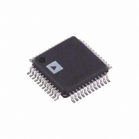
ADAU1328BSTZ Analog Devices Inc, ADAU1328BSTZ Datasheet - Page 24

ADAU1328BSTZ
Manufacturer Part Number
ADAU1328BSTZ
Description
IC CODEC 24BIT 2ADC/8DAC 48LQFP
Manufacturer
Analog Devices Inc
Type
General Purposer
Datasheet
1.ADAU1328BSTZ-RL.pdf
(32 pages)
Specifications of ADAU1328BSTZ
Data Interface
Serial
Resolution (bits)
24 b
Number Of Adcs / Dacs
2 / 8
Sigma Delta
Yes
S/n Ratio, Adcs / Dacs (db) Typ
94 / 94
Dynamic Range, Adcs / Dacs (db) Typ
105 / 106
Voltage - Supply, Analog
3 V ~ 3.6 V
Voltage - Supply, Digital
3 V ~ 3.6 V
Operating Temperature
-40°C ~ 85°C
Mounting Type
Surface Mount
Package / Case
48-LQFP
Audio Codec Type
Stereo
No. Of Adcs
2
No. Of Dacs
8
No. Of Input Channels
2
No. Of Output Channels
8
Adc / Dac Resolution
24bit
Adcs / Dacs Signal To Noise Ratio
108dB
Lead Free Status / RoHS Status
Lead free / RoHS Compliant
Available stocks
Company
Part Number
Manufacturer
Quantity
Price
Company:
Part Number:
ADAU1328BSTZ
Manufacturer:
ADI
Quantity:
150
Company:
Part Number:
ADAU1328BSTZ
Manufacturer:
Analog Devices Inc
Quantity:
10 000
Company:
Part Number:
ADAU1328BSTZ-RL
Manufacturer:
Analog Devices Inc
Quantity:
10 000
ADAU1328
CONTROL REGISTERS
DEFINITIONS
The format is the same for I
in I
DAC volume registers that are set to full volume.
Note that the first setting in each control register parameter is the default setting.
Table 13. Register Format
Bit
Table 14. Register Addresses and Functions
Address
0
1
2
3
4
5
6
7
8
9
10
11
12
13
14
15
16
PLL AND CLOCK CONTROL REGISTERS
Table 15. PLL and Clock Control 0
Bit
0
2:1
4:3
6:5
7
2
C, ADR0 and ADR1 are OR’ e d into Bit 17 and Bit 8 to provide multiple chip addressing. All registers are reset to 0, except for the
Global Address
23:17
Value
0
1
00
01
10
11
00
01
10
11
00
01
10
11
0
1
Function
PLL and Clock Control 0
PLL and Clock Control 1
DAC Control 0
DAC Control 1
DAC Control 2
DAC individual channel mutes
DAC 1L volume control
DAC 1R volume control
DAC 2L volume control
DAC 2R volume control
DAC 3L volume control
DAC 3R volume control
DAC 4L volume control
DAC 4R volume control
ADC Control 0
ADC Control 1
ADC Control 2
Function
Normal operation
Power-down
INPUT 256 (×44.1 kHz or 48 kHz)
INPUT 384 (×44.1 kHz or 48 kHz)
INPUT 512 (×44.1 kHz or 48 kHz)
INPUT 768 (×44.1 kHz or 48 kHz)
XTAL oscillator enabled
256 × f
512 × f
Off
MCLK
DLRCLK
ALRCLK
Reserved
Disable: ADC and DAC idle
Enable: ADC and DAC active
2
C and SPI ports. The global address for the ADAU1328 is 0x04, shifted left 1 bit due to the R/ W bit. However,
S
S
VCO output
VCO output
R/W
16
Rev. 0 | Page 24 of 32
Description
PLL power-down
MCLK pin functionality (PLL active)
MCLKO pin
PLL input
Internal MCLK enable
Register Address
15:8
Data
7:0


