SJA1000T/N1,118 NXP Semiconductors, SJA1000T/N1,118 Datasheet - Page 52
SJA1000T/N1,118
Manufacturer Part Number
SJA1000T/N1,118
Description
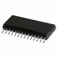
IC STAND-ALONE CAN CTRLR 28-SOIC
Manufacturer
NXP Semiconductors
Datasheet
1.SJA1000TN1112.pdf
(68 pages)
Specifications of SJA1000T/N1,118
Package / Case
28-SOIC (7.5mm Width)
Controller Type
CAN Interface
Interface
CAN
Voltage - Supply
4.5 V ~ 5.5 V
Current - Supply
15mA
Operating Temperature
-40°C ~ 125°C
Mounting Type
Surface Mount
Product
Controller Area Network (CAN)
Number Of Transceivers
1
Data Rate
1 Mbps
Frequency
24 MHz
Supply Voltage (max)
5.5 V
Supply Voltage (min)
4.5 V
Supply Current (max)
15 mA
Maximum Operating Temperature
+ 125 C
Minimum Operating Temperature
- 40 C
Mounting Style
SMD/SMT
Package
28SO
Maximum Data Rate
1 Mbps
Minimum Single Supply Voltage
4.5 V
Standard Supported
CAN 2.0B
Power Down Mode
Sleep
Maximum Single Supply Voltage
5.5 V
Lead Free Status / RoHS Status
Lead free / RoHS Compliant
Lead Free Status / RoHS Status
Lead free / RoHS Compliant, Lead free / RoHS Compliant
Other names
568-1123-2
935230920118
SJA1000TD-T
935230920118
SJA1000TD-T
Available stocks
Company
Part Number
Manufacturer
Quantity
Price
Company:

Part Number:
SJA1000T/N1,118
Manufacturer:
XILINX
Quantity:
125
Part Number:
SJA1000T/N1,118
Manufacturer:
NXP/恩智浦
Quantity:
20 000


Philips Semiconductors
If the SJA1000 is in the sleep mode a recessive level is output on the TX0 and TX1 pins with respect to the contents
within the output control register. If the SJA1000 is in the reset state (reset request = HIGH) or the external reset pin RST
is pulled LOW the outputs TX0 and TX1 are floating.
The transmit output stage is able to operate in different modes. Table 47 shows the output control register settings.
Table 47 Interpretation of OCMODE bits
Note
1. In test output mode TXn will reflect the bit, detected on RX pins, with the next positive edge of the system clock.
6.5.3.1
In normal output mode the bit sequence (TXD) is sent via TX0 and TX1. The voltage levels on the output driver pins TX0
and TX1 depend on both the driver characteristic programmed by OCTPx, OCTNx (float, pull-up, pull-down, push-pull)
and the output polarity programmed by OCPOLx.
2000 Jan 04
handbook, full pagewidth
OCMODE1
Stand-alone CAN controller
TN1, TN0, TP1 and TP0 are configured in accordance with the setting of OCR.
0
0
1
1
Normal output mode
OCMODE0
0
1
0
1
bi-phase output mode
test output mode; note 1
normal output mode
clock output mode
TXCLK
TXD
OCTP1
OCTN1
OCPOL1
OCTP0
OCTN0
OCPOL0
OCMODE1
OCMODE0
Fig.14 Transceiver input/output control logic.
TRANSMIT
LOGIC
52
DESCRIPTION
V DD
V DD
V SS
V SS
TP0
TN0
TP1
TN1
MGK629
TX0
TX1
transmitter
Product specification
SJA1000
Related parts for SJA1000T/N1,118
Image
Part Number
Description
Manufacturer
Datasheet
Request
R

Part Number:
Description:
IC STAND-ALONE CAN CTRLR 28-SOIC
Manufacturer:
NXP Semiconductors
Datasheet:

Part Number:
Description:
Manufacturer:
NXP Semiconductors
Datasheet:
Part Number:
Description:
IC STAND-ALONE CAN CTRLR 28-SOIC
Manufacturer:
NXP Semiconductors
Datasheet:
Part Number:
Description:
IC STAND-ALONE CAN CTRLR 28-SOIC
Manufacturer:
NXP Semiconductors
Datasheet:
Part Number:
Description:
Manufacturer:
NXP Semiconductors
Datasheet:
Part Number:
Description:
Manufacturer:
NXP Semiconductors
Datasheet:
Part Number:
Description:
Manufacturer:
NXP Semiconductors
Datasheet:

Part Number:
Description:
CONTROLLER, CAN, STANDALONE, 28SOIC
Manufacturer:
NXP Semiconductors
Datasheet:
Part Number:
Description:
Stand-alone Can Controller
Manufacturer:
NXP Semiconductors
Datasheet:
Part Number:
Description:
Network Controller & Processor ICs STAND ALONE CAN CONTROLLER
Manufacturer:
NXP Semiconductors
Datasheet:
Part Number:
Description:
NXP Semiconductors designed the LPC2420/2460 microcontroller around a 16-bit/32-bitARM7TDMI-S CPU core with real-time debug interfaces that include both JTAG andembedded trace
Manufacturer:
NXP Semiconductors
Datasheet:

Part Number:
Description:
NXP Semiconductors designed the LPC2458 microcontroller around a 16-bit/32-bitARM7TDMI-S CPU core with real-time debug interfaces that include both JTAG andembedded trace
Manufacturer:
NXP Semiconductors
Datasheet:
Part Number:
Description:
NXP Semiconductors designed the LPC2468 microcontroller around a 16-bit/32-bitARM7TDMI-S CPU core with real-time debug interfaces that include both JTAG andembedded trace
Manufacturer:
NXP Semiconductors
Datasheet:
Part Number:
Description:
NXP Semiconductors designed the LPC2470 microcontroller, powered by theARM7TDMI-S core, to be a highly integrated microcontroller for a wide range ofapplications that require advanced communications and high quality graphic displays
Manufacturer:
NXP Semiconductors
Datasheet:
Part Number:
Description:
NXP Semiconductors designed the LPC2478 microcontroller, powered by theARM7TDMI-S core, to be a highly integrated microcontroller for a wide range ofapplications that require advanced communications and high quality graphic displays
Manufacturer:
NXP Semiconductors
Datasheet: