SJA1000T/N1,118 NXP Semiconductors, SJA1000T/N1,118 Datasheet - Page 56
SJA1000T/N1,118
Manufacturer Part Number
SJA1000T/N1,118
Description
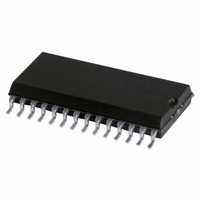
IC STAND-ALONE CAN CTRLR 28-SOIC
Manufacturer
NXP Semiconductors
Datasheet
1.SJA1000TN1112.pdf
(68 pages)
Specifications of SJA1000T/N1,118
Package / Case
28-SOIC (7.5mm Width)
Controller Type
CAN Interface
Interface
CAN
Voltage - Supply
4.5 V ~ 5.5 V
Current - Supply
15mA
Operating Temperature
-40°C ~ 125°C
Mounting Type
Surface Mount
Product
Controller Area Network (CAN)
Number Of Transceivers
1
Data Rate
1 Mbps
Frequency
24 MHz
Supply Voltage (max)
5.5 V
Supply Voltage (min)
4.5 V
Supply Current (max)
15 mA
Maximum Operating Temperature
+ 125 C
Minimum Operating Temperature
- 40 C
Mounting Style
SMD/SMT
Package
28SO
Maximum Data Rate
1 Mbps
Minimum Single Supply Voltage
4.5 V
Standard Supported
CAN 2.0B
Power Down Mode
Sleep
Maximum Single Supply Voltage
5.5 V
Lead Free Status / RoHS Status
Lead free / RoHS Compliant
Lead Free Status / RoHS Status
Lead free / RoHS Compliant, Lead free / RoHS Compliant
Other names
568-1123-2
935230920118
SJA1000TD-T
935230920118
SJA1000TD-T
Available stocks
Company
Part Number
Manufacturer
Quantity
Price
Company:

Part Number:
SJA1000T/N1,118
Manufacturer:
XILINX
Quantity:
125
Part Number:
SJA1000T/N1,118
Manufacturer:
NXP/恩智浦
Quantity:
20 000


Philips Semiconductors
6.5.4.1
The bits CD.2 to CD.0 are accessible without restrictions in reset mode as well as in operating mode. These bits are used
to define the frequency at the external CLKOUT pin. For an overview of selectable frequencies see Table 50.
Table 50 CLKOUT frequency selection; note 1
Note
1. f
6.5.4.2
Setting this bit allows the external CLKOUT pin of the
SJA1000 to be disabled. A write access is possible only in
reset mode. If this bit is set, CLKOUT is LOW during sleep
mode, otherwise it is HIGH.
6.5.4.3
This bit allows the TX1 output to be used as a dedicated
receive interrupt output. When a received message has
passed the acceptance filter successfully, a receive
interrupt pulse with the length of one bit time is always
output at the TX1 pin (during the last bit of end of frame).
The transmit output stage should operate in normal output
mode. The polarity and output drive are programmable via
the output control register (see also Section 6.5.3). A write
access is only possible in reset mode.
2000 Jan 04
Stand-alone CAN controller
osc
CD.2
0
0
0
0
1
1
1
1
is the frequency of the external oscillator (XTAL).
CD.2 to CD.0
Clock off
RXINTEN
CD.1
0
0
1
1
0
0
1
1
CD.0
0
1
0
1
0
1
0
1
f
f
--------
f
--------
f
--------
f
--------
f
--------
f
--------
osc
f
--------
12
14
10
osc
osc
osc
osc
osc
osc
osc
2
4
6
8
56
6.5.4.4
Setting of CDR.6 allows to bypass the CAN input
comparator and is only possible in reset mode. This is
useful in the event that the SJA1000 is connected to an
external transceiver circuit. The internal delay of the
SJA1000 is reduced, which will result in a longer maximum
possible bus length. If CBP is set, only RX0 is active. The
unused RX1 input should be connected to a defined level
(e.g. V
6.5.4.5
CDR.7 defines the CAN mode. If CDR.7 is at logic 0 the
CAN controller operates in BasicCAN mode. If set to
logic 1 the CAN controller operates in PeliCAN mode.
Write access is only possible in reset mode.
SS
).
CBP
CAN mode
CLKOUT FREQUENCY
Product specification
SJA1000
Related parts for SJA1000T/N1,118
Image
Part Number
Description
Manufacturer
Datasheet
Request
R

Part Number:
Description:
IC STAND-ALONE CAN CTRLR 28-SOIC
Manufacturer:
NXP Semiconductors
Datasheet:

Part Number:
Description:
Manufacturer:
NXP Semiconductors
Datasheet:
Part Number:
Description:
IC STAND-ALONE CAN CTRLR 28-SOIC
Manufacturer:
NXP Semiconductors
Datasheet:
Part Number:
Description:
IC STAND-ALONE CAN CTRLR 28-SOIC
Manufacturer:
NXP Semiconductors
Datasheet:
Part Number:
Description:
Manufacturer:
NXP Semiconductors
Datasheet:
Part Number:
Description:
Manufacturer:
NXP Semiconductors
Datasheet:
Part Number:
Description:
Manufacturer:
NXP Semiconductors
Datasheet:

Part Number:
Description:
CONTROLLER, CAN, STANDALONE, 28SOIC
Manufacturer:
NXP Semiconductors
Datasheet:
Part Number:
Description:
Stand-alone Can Controller
Manufacturer:
NXP Semiconductors
Datasheet:
Part Number:
Description:
Network Controller & Processor ICs STAND ALONE CAN CONTROLLER
Manufacturer:
NXP Semiconductors
Datasheet:
Part Number:
Description:
NXP Semiconductors designed the LPC2420/2460 microcontroller around a 16-bit/32-bitARM7TDMI-S CPU core with real-time debug interfaces that include both JTAG andembedded trace
Manufacturer:
NXP Semiconductors
Datasheet:

Part Number:
Description:
NXP Semiconductors designed the LPC2458 microcontroller around a 16-bit/32-bitARM7TDMI-S CPU core with real-time debug interfaces that include both JTAG andembedded trace
Manufacturer:
NXP Semiconductors
Datasheet:
Part Number:
Description:
NXP Semiconductors designed the LPC2468 microcontroller around a 16-bit/32-bitARM7TDMI-S CPU core with real-time debug interfaces that include both JTAG andembedded trace
Manufacturer:
NXP Semiconductors
Datasheet:
Part Number:
Description:
NXP Semiconductors designed the LPC2470 microcontroller, powered by theARM7TDMI-S core, to be a highly integrated microcontroller for a wide range ofapplications that require advanced communications and high quality graphic displays
Manufacturer:
NXP Semiconductors
Datasheet:
Part Number:
Description:
NXP Semiconductors designed the LPC2478 microcontroller, powered by theARM7TDMI-S core, to be a highly integrated microcontroller for a wide range ofapplications that require advanced communications and high quality graphic displays
Manufacturer:
NXP Semiconductors
Datasheet: