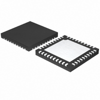
SI3452A-B01-GM Silicon Laboratories Inc, SI3452A-B01-GM Datasheet - Page 15

SI3452A-B01-GM
Manufacturer Part Number
SI3452A-B01-GM
Description
IC POE CONTROLLER MIDSPAN 40QFN
Manufacturer
Silicon Laboratories Inc
Datasheet
1.SI3452B-B01-GM.pdf
(36 pages)
Specifications of SI3452A-B01-GM
Package / Case
40-QFN
Controller Type
Power over Ethernet Controller (POE)
Interface
I²C
Voltage - Supply
3 V ~ 3.6 V
Current - Supply
14mA
Operating Temperature
-40°C ~ 85°C
Mounting Type
Surface Mount
Maximum Power Dissipation
1.2 W
Minimum Operating Temperature
- 40 C
Mounting Style
SMD/SMT
Product
Ethernet Controllers
Standard Supported
IEEE 802.3at, IEEE 802.3af
Supply Voltage (max)
3.6 V
Supply Voltage (min)
3 V
Supply Current (max)
14 mA
Maximum Operating Temperature
+ 85 C
Lead Free Status / RoHS Status
Lead free / RoHS Compliant
Lead Free Status / RoHS Status
Lead free / RoHS Compliant, Lead free / RoHS Compliant
Other names
336-1831-5
Available stocks
Company
Part Number
Manufacturer
Quantity
Price
Company:
Part Number:
SI3452A-B01-GM
Manufacturer:
SILICON
Quantity:
1 001
Company:
Part Number:
SI3452A-B01-GMR
Manufacturer:
SILICON
Quantity:
670
4.8. SMBus/I
The I
Specification (SMBus), version 1.1 and compatible with the I
system controller are byte-oriented with the I
method of extending the clock-low duration is available to accommodate devices with different speed capabilities
on the same bus. The I
arbitration logic, and START/STOP control and generation.
A typical I
Bit0: R/W direction bit), one or more bytes of data, and a STOP condition. Each byte that is received (by a master
or slave) must be acknowledged (ACK) with a low SDA during a high SCL (see Figure 6). If the receiving device
does not ACK, the transmitting device will read a NACK (not acknowledge), which is a high SDA during a high
SCL.
The direction bit (R/W) occupies the least-significant bit position of the address byte. The direction bit is set to logic
1 to indicate a "READ" operation and cleared to logic 0 to indicate a "WRITE" operation. All transactions are
initiated by a master, with one or more addressed slave devices as the target. The master generates the START
condition and then transmits the slave address and direction bit. If the transaction is a WRITE operation from the
master to the slave, the master transmits the data one byte at a time, waiting for an ACK from the slave at the end
of each byte.
For READ operations, the slave transmits the data waiting for an ACK from the master at the end of each byte. At
the end of the data transfer, the master generates a STOP condition to terminate the transaction and free the bus.
Figure 6 illustrates a typical SMBus/I
Silicon Laboratories recommends the use of bidirectional digital isolators, such as the Si840x, to isolate the I
communications interface between the Si3452 high-voltage port controllers and the system host controller.
The Si3452 does not support the alert response address (ARA) protocol. Polling is used to determine which
controller is interrupting in an interrupt-driven system.
START
ST ART
2
C interface is a two-wire, bidirectional serial bus. The I
0
0
F ixed IC
Address
Fixed IC
Addr ess
2
C transaction consists of a START condition followed by an address byte (Bits7–1: 7-bit slave address;
1
1
0
0
Slave Address
Slave Addr ess
2
A3 A2 A1 A0 R/W#
A3 A2 A1 A0 R/W#
C Interface Description
Pin Set IC
Pin Set IC
Addr ess
Address
2
C provides control of SDA (serial data), SCL (serial clock) generation and synchronization,
ACK by IC
ACK by IC
Setup Register Addr ess
A7 A6 A5 A4
A7
Figure 6. Typical I
2
A6 A5 A4 A3 A2 A1 A0
C transaction.
Register Address
Register Address
2
A3 A2 A1 A0
C interface autonomously controlling the serial transfer of the data. A
Read Sequence
Write Sequence
ACK by IC
ACK by IC
Rev. 1.2
START
2
C Bus Transactions
D7 D6 D5 D4 D3 D2 D1 D0
2
C serial bus. Reads and writes to the interface by the
F ixed IC
Address
0
2
C is compliant with the System Management Bus
1
Write Data
0
Slave Address
A3 A2 A1 A0 R/W#
Pin Set IC
Addr ess
ACK by IC
ACK by IC
Transfer Data to Setup Address
ST OP by Master
D7 D6 D5 D4 D3 D2 D1 D0
Register Data
Not ACK by Master
Si3452
STOP by Master
2
15
C


