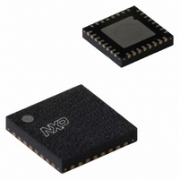
MFRC52201HN1,157 NXP Semiconductors, MFRC52201HN1,157 Datasheet - Page 27

MFRC52201HN1,157
Manufacturer Part Number
MFRC52201HN1,157
Description
IC SMART CARD READER
Manufacturer
NXP Semiconductors
Datasheet
1.MFRC52201HN1157.pdf
(109 pages)
Specifications of MFRC52201HN1,157
Controller Type
Smart Card Interface
Interface
SPI
Voltage - Supply
1.6 V ~ 3.6 V
Current - Supply
60mA
Operating Temperature
-25°C ~ 85°C
Mounting Type
Surface Mount
Package / Case
32-VQFN Exposed Pad, 32-HVQFN, 32-SQFN, 32-DHVQFN
Lead Free Status / RoHS Status
Lead free / RoHS Compliant
Other names
935280547157
MFRC52201HN1
MFRC52201HN1
MFRC52201HN1
MFRC52201HN1
- Current page: 27 of 109
- Download datasheet (3Mb)
NXP Semiconductors
112132
Product data sheet
9.2.2.5 TxControlReg
Table 46:
Controls the logical behavior of the antenna driver pins Tx1 and Tx2.
Table 47:
Table 48:
Bit
3
2
1 to 0
Bit
7
6
5
4
3
2
1
0
Symbol
Access
Rights
Bit
InvTx2RF
Symbol
RxNoErr
RxMultiple
-
Symbol
InvTx2RFOn
InvTx1RFOn
InvTx2RFOff
InvTx1RFOff
Tx2CW
-
Tx2RFEn
Tx1RFEn
Description of RxModeReg bits
Description of TxControlReg bits
TxControlReg register (address 14h); reset value: 80h
On
r/w
7
InvTx1RF
Rev. 3.2 — 22 May 2007
r/w
Description
If set to logic 1, a not valid received data stream (less than 4 bits
received) will be ignored. The receiver will remain active.
Set to logic 0, the receiver is deactivated after receiving a data frame.
Set to logic 1, it is possible to receive more than one data frame. This bit
is only valid for data rates above 106 kbit/s to handle the Polling
command. Having set this bit, the receive and transceive commands will
not terminate automatically. In this case the multiple receiving can only
be deactivated by writing any command (except the Receive command)
to the CommandReg register or by clearing the bit by the host.
If set to logic 1, at the end of a received data stream an error byte is
added to the FIFO. The error byte is a copy of the ErrorReg register.
Reserved for future use.
On
6
Description
Set to logic 1, the output signal at pin TX2 will be inverted, if driver TX2
is enabled.
Set to logic 1, the output signal at pin TX1 will be inverted, if driver TX1
is enabled.
Set to logic 1, the output signal at pin TX2 will be inverted, if driver TX2
is disabled.
Set to logic 1, the output signal at pin TX1 will be inverted, if driver TX1
is disabled.
Set to logic 1, the output signal on pin TX2 will deliver continuously the
un-modulated 13.56 MHz energy carrier.
Set to logic 0, Tx2CW is enabled to modulate the 13.56 MHz energy
carrier.
Reserved for future use.
Set to logic 1, the output signal on pin TX2 will deliver the 13.56 MHz
energy carrier modulated by the transmission data.
Set to logic 1, the output signal on pin TX1 will deliver the 13.56 MHz
energy carrier modulated by the transmission data.
InvTx2RF
r/w
Off
5
…continued
InvTx1RF
Off
r/w
4
Tx2CW
r/w
3
RFU
2
-
Contactless Reader IC
MFRC522
Tx2RFEn Tx1RFEn
© NXP B.V. 2007. All rights reserved.
r/w
1
27 of 109
r/w
0
Related parts for MFRC52201HN1,157
Image
Part Number
Description
Manufacturer
Datasheet
Request
R
Part Number:
Description:
Contactless Reader Ic
Manufacturer:
NXP Semiconductors
Datasheet:
Part Number:
Description:
NXP Semiconductors designed the LPC2420/2460 microcontroller around a 16-bit/32-bitARM7TDMI-S CPU core with real-time debug interfaces that include both JTAG andembedded trace
Manufacturer:
NXP Semiconductors
Datasheet:

Part Number:
Description:
NXP Semiconductors designed the LPC2458 microcontroller around a 16-bit/32-bitARM7TDMI-S CPU core with real-time debug interfaces that include both JTAG andembedded trace
Manufacturer:
NXP Semiconductors
Datasheet:
Part Number:
Description:
NXP Semiconductors designed the LPC2468 microcontroller around a 16-bit/32-bitARM7TDMI-S CPU core with real-time debug interfaces that include both JTAG andembedded trace
Manufacturer:
NXP Semiconductors
Datasheet:
Part Number:
Description:
NXP Semiconductors designed the LPC2470 microcontroller, powered by theARM7TDMI-S core, to be a highly integrated microcontroller for a wide range ofapplications that require advanced communications and high quality graphic displays
Manufacturer:
NXP Semiconductors
Datasheet:
Part Number:
Description:
NXP Semiconductors designed the LPC2478 microcontroller, powered by theARM7TDMI-S core, to be a highly integrated microcontroller for a wide range ofapplications that require advanced communications and high quality graphic displays
Manufacturer:
NXP Semiconductors
Datasheet:
Part Number:
Description:
The Philips Semiconductors XA (eXtended Architecture) family of 16-bit single-chip microcontrollers is powerful enough to easily handle the requirements of high performance embedded applications, yet inexpensive enough to compete in the market for hi
Manufacturer:
NXP Semiconductors
Datasheet:
Part Number:
Description:
The XA-S3 device is a member of Philips Semiconductors? XA(eXtended Architecture) family of high performance 16-bitsingle-chip microcontrollers
Manufacturer:
NXP Semiconductors
Datasheet:

Part Number:
Description:
The NXP BlueStreak LH75401/LH75411 family consists of two low-cost 16/32-bit System-on-Chip (SoC) devices
Manufacturer:
NXP Semiconductors
Datasheet:

Part Number:
Description:
The NXP LPC3130/3131 combine an 180 MHz ARM926EJ-S CPU core, high-speed USB2
Manufacturer:
NXP Semiconductors
Datasheet:

Part Number:
Description:
The NXP LPC3141 combine a 270 MHz ARM926EJ-S CPU core, High-speed USB 2
Manufacturer:
NXP Semiconductors

Part Number:
Description:
The NXP LPC3143 combine a 270 MHz ARM926EJ-S CPU core, High-speed USB 2
Manufacturer:
NXP Semiconductors

Part Number:
Description:
The NXP LPC3152 combines an 180 MHz ARM926EJ-S CPU core, High-speed USB 2
Manufacturer:
NXP Semiconductors

Part Number:
Description:
The NXP LPC3154 combines an 180 MHz ARM926EJ-S CPU core, High-speed USB 2
Manufacturer:
NXP Semiconductors


