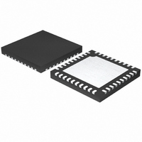
SI3452D-B01-GM Silicon Laboratories Inc, SI3452D-B01-GM Datasheet - Page 13

SI3452D-B01-GM
Manufacturer Part Number
SI3452D-B01-GM
Description
IC POE CONTROLLER MIDSPAN 40QFN
Manufacturer
Silicon Laboratories Inc
Datasheet
1.SI3452B-B01-GM.pdf
(36 pages)
Specifications of SI3452D-B01-GM
Package / Case
40-QFN
Controller Type
Power over Ethernet Controller (POE)
Interface
I²C
Voltage - Supply
3 V ~ 3.6 V
Current - Supply
14mA
Operating Temperature
-40°C ~ 85°C
Mounting Type
Surface Mount
Maximum Power Dissipation
1.2 W
Minimum Operating Temperature
- 40 C
Mounting Style
SMD/SMT
Product
Ethernet Controllers
Standard Supported
IEEE 802.3at, IEEE 802.3af
Supply Voltage (max)
3.6 V
Supply Voltage (min)
3 V
Supply Current (max)
14 mA
Maximum Operating Temperature
+ 85 C
Lead Free Status / RoHS Status
Lead free / RoHS Compliant
Lead Free Status / RoHS Status
Lead free / RoHS Compliant, Lead free / RoHS Compliant
Other names
336-1835-5
Available stocks
Company
Part Number
Manufacturer
Quantity
Price
Company:
Part Number:
SI3452D-B01-GM
Manufacturer:
Silicon Labs
Quantity:
135
Si3452
4.2. Classification
Following a successful PD detection, the classification phase will be automatically initiated in all operational
modes. During this phase, a single measurement will be made at 18 V to determine how much power the PD
device will draw under maximum loads per the IEEE 802.3af and 802.3at standards. The current limit during this
test mode is 60 mA nominal.
The Si3452 supports 1-Event and 2-Event classification. When operating in PoE (<15.4 W) mode, 1-Event
classification is used. Operation in PoE+ (>15.4 W) mode results in 2-Event classification probes. The 1-Event
classification is compliant to IEEE standard 802.3-2005. 2-Event classification is compliant to draft IEEE P802.3at.
4.3. Port Turn-On and Power FETs
The FET is turned on with a gate drive that results in a very low-noise turn-on waveform with a slew rate of less
than 1 V/µsec (See Figure 5).
The power FET switch on each port has been sized to have a typical ON resistance of approximately 0.3 . The
shunt resistor for current measurement has also been set to 0.1 . Including interconnection and process variation,
the total resistance to VEE for a port that is on is 0.6 (max). This limits the maximum power dissipation per
channel to < 250 mW when the operating current is 600 mA, the maximum current allowed by the IEEE 802.3at
PoE+ standard.
The FET has a programmable operating current limit. Each channel can be set to support output currents of
400 mA or 800 mA minimum.
In addition to the normal current limit, there is a short circuit current shutdown approximately 25% greater than the
nominal current limit. If there is a transient current surge where the current ramps up faster than the programmed
current limit can respond, the gate drive voltage is clamped immediately to V
. The clamp is enabled for at least
EE
10 µs, which allows the normal current circuitry to respond.
Another important protection feature is foldback current limiting. When V
is near V
, the current limit is at
OUT
EE
maximum. As the V
of the driver switch increases (and V
is closer to ground), the current limit goes to its
DS
OUT
lowest level. The amount of the foldback current is scaled proportionally with the programmed current limit.
Figure 5. Turn-On Waveform—Vport Relative to GND
Rev. 1.2
13


