DP83907VF National Semiconductor, DP83907VF Datasheet - Page 14
DP83907VF
Manufacturer Part Number
DP83907VF
Description
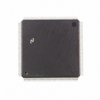
IC CONTROLLR AT/LANII TP 160PQFP
Manufacturer
National Semiconductor
Datasheet
1.DP83907VF.pdf
(70 pages)
Specifications of DP83907VF
Controller Type
Network Interface Controller (NIC)
Interface
Twisted Pair
Voltage - Supply
4.75 V ~ 5.25 V
Current - Supply
150mA
Operating Temperature
0°C ~ 70°C
Mounting Type
Surface Mount
Package / Case
160-MQFP, 160-PQFP
Lead Free Status / RoHS Status
Contains lead / RoHS non-compliant
Other names
*DP83907VF
Available stocks
Company
Part Number
Manufacturer
Quantity
Price
Company:

Part Number:
DP83907VF
Manufacturer:
NSC
Quantity:
5 510


4 0 Functional Description
ing the last transmit byte During reception the CRC logic
generates a CRC field from the incoming packet This local
CRC is serially compared to the incoming CRC appended to
the end of the packet by the transmitting node If the local
and received CRC match a specific pattern will be generat-
ed and decoded to indicate no data errors Transmission
errors result in different pattern and are detected resulting
in rejection of a packet
Transmit Serializer
The Transmit Serializer reads parallel data from the FIFO
and serializes it for transmission The serializer is clocked by
the transmit clock generated internally The serial data is
also shifted into the CRC generator checker At the begin-
ning of each transmission the Preamble and SFD Genera-
tor append 62 bits of 1 0 preamble and a 1 1 synch pattern
After the last data byte of the packet has been serialized the
32-bit FCS (Frame Check Sequence) field is shifted directly
out of the CRC generator In the event of a collision the
Preamble and SFD generator is used to generate a 32-bit
JAM pattern of all 1’s
Comparator-Address Recognition Logic
The address recognition logic compares the Destination Ad-
dress Field (first 6 bytes of the received packet) to the Phys-
ical address registers stored in the Address Register Array
FIGURE 12 DP8390 Core Simplified Block Diagram
(Continued)
14
If any one of the six bytes does not match the pre-pro-
grammed physical address the Protocol Control Logic re-
jects the packet All multicast destination addresses are fil-
tered using a hashing technique (See register description )
If the multicast address indexes a bit that has been set in
the filter bit array of the Multicast Address Register Array
the packet is accepted otherwise it is rejected by the Proto-
col Control Logic Each destination address is also checked
for all 1’s which is the reserved broadcast address
FIFO and Packet Data Operations
OVERVIEW
To accommodate the different rates at which data comes
from (or goes to) the network and goes to (or comes from)
the packet buffer memory the DP83907 contains a 16-byte
FIFO for buffering data between the media and the buffer
RAM located on the memory support bus The FIFO thresh-
old is programmable When the FIFO has filled to its pro-
grammed threshold the local DMA channel transfers these
bytes (or words) into local memory (via the memory bus) It
is crucial that the local DMA is given access to the bus
within a minimum bus latency time otherwise a FIFO under-
run (or overrun) occurs
TL F 12082 – 7
Related parts for DP83907VF
Image
Part Number
Description
Manufacturer
Datasheet
Request
R

Part Number:
Description:
NIC Network Interface Controller
Manufacturer:
NSC [National Semiconductor]
Datasheet:

Part Number:
Description:
National Semiconductor [8-Bit D/A Converter]
Manufacturer:
National Semiconductor
Datasheet:
Part Number:
Description:
National Semiconductor [Media Coprocessor]
Manufacturer:
National Semiconductor
Datasheet:
Part Number:
Description:
Digitally Controlled Tone and Volume Circuit with Stereo Audio Power Amplifier, Microphone Preamp Stage and National 3D Sound
Manufacturer:
National Semiconductor
Datasheet:
Part Number:
Description:
Digitally Controlled Tone and Volume Circuit with Stereo Audio Power Amplifier, Microphone Preamp Stage and National 3D Sound
Manufacturer:
National Semiconductor
Datasheet:
Part Number:
Description:
AC97 Rev 2 Codec with Sample Rate Conversion and National 3D Sound
Manufacturer:
National Semiconductor
Part Number:
Description:
Manufacturer:
National Semiconductor
Datasheet:
Part Number:
Description:
Manufacturer:
National Semiconductor
Datasheet:
Part Number:
Description:
General Purpose, Low Voltage, Low Power, Rail-to-Rail Output Operational Amplifiers
Manufacturer:
National Semiconductor
Datasheet:
Part Number:
Description:
8-bit 20 MSPS flash A/D converter.
Manufacturer:
National Semiconductor
Datasheet:
Part Number:
Description:
Low Noise Quad Operational Amplifier
Manufacturer:
National Semiconductor
Datasheet:
Part Number:
Description:
Quad Differential Line Receivers
Manufacturer:
National Semiconductor
Datasheet:
Part Number:
Description:
Quad High Speed Trapezoidal? Bus Transceiver
Manufacturer:
National Semiconductor
Datasheet:
Part Number:
Description:
Dual Line Receiver
Manufacturer:
National Semiconductor
Datasheet: