CY7C68001-56PVXC Cypress Semiconductor Corp, CY7C68001-56PVXC Datasheet - Page 44
CY7C68001-56PVXC
Manufacturer Part Number
CY7C68001-56PVXC
Description
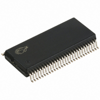
IC USB INTERFACE SX2 56-SSOP
Manufacturer
Cypress Semiconductor Corp
Type
USBr
Series
CY7Cr
Datasheet
1.CY7C68001-56PVXC.pdf
(45 pages)
Specifications of CY7C68001-56PVXC
Package / Case
56-SSOP
Protocol
USB 2.0
Voltage - Supply
3 V ~ 3.6 V
Mounting Type
Surface Mount
Maximum Operating Temperature
+ 70 C
Minimum Operating Temperature
0 C
Mounting Style
SMD/SMT
Operating Temperature Range
0 C to + 70 C
Operating Supply Voltage
3.3 V
Core Size
8 Bit
No. Of I/o's
35
Ram Memory Size
256Byte
Embedded Interface Type
SPI, USB
Digital Ic Case Style
SSOP
Supply Voltage Range
3V To 3.6V
Rohs Compliant
Yes
Lead Free Status / RoHS Status
Lead free / RoHS Compliant
Number Of Drivers/receivers
-
Lead Free Status / Rohs Status
Lead free / RoHS Compliant
Other names
428-1864
CY7C68001-56PVXC
CY7C68001-56PVXC
Available stocks
Company
Part Number
Manufacturer
Quantity
Price
Company:

Part Number:
CY7C68001-56PVXC
Manufacturer:
CY
Quantity:
101
Company:
Part Number:
CY7C68001-56PVXC
Manufacturer:
CYPRESS
Quantity:
7
Part Number:
CY7C68001-56PVXC
Manufacturer:
CYPRESS/赛普拉斯
Quantity:
20 000


Document #: 38-08013 Rev. *J
Description Title: CY7C68001 EZ-USB SX2™ High Speed USB Interface Device
Document Number: 38-08013
*D
*G
*H
*E
*F
*J
*I
2665531
2733374
130447
243316
329238
392570
411515
02/26/2009
07/08/2009
See ECN
See ECN
See ECN
See ECN
12/17/03
ANTG/AESA Updated cross-references on pages 2 and 3
DPT/PYRS Added package diagram (51-85187) and updated Ordering Information table.
KKU
KKU
KEV
KEV
BHA
Provided additional timing restrictions and requirement regarding the use of
Modified
Replaced package diagram in
Fixed last history entry for rev *C
Change reference in section 2.7.2.4 from XXXXXXX to 7.3
Removed the word “compatible” in section 3.3
Change the text in section 5.0, last paragraph from 0xE6FB to 0xE683
Changed label “Reset” to “Default” in sections 5.1 and 7.2 through 7.14
Reformatted Figure 4
Added entries 3A, 3B, 3C, 0xE609, and 0xE683 to
Change access on hex values 07 and 09 from bbbbbbbb to bbbbrbrr
Removed t
Corrected timing diagrams, figures 11-1,11-2, 11-6
Changed
reference to t3 which should be t2, added reference of t3 for deasserting SLWR and
reworded section 11.6
Updated I
Reformatted data sheet to latest format
Added Lead-free parts numbers
Updated default value for address 0x07 and 0x09
Added Footnote 3.
Removed requirement of less then 360 nsec period between nibble writes in
command
Changed PKTEND to FLAGS output propagation delay in table 11-16 from a max
value of 70 ns to 110 ns
PKTEND pin to commit a short one byte/word packet subsequent to committing a
packet automatically (when in auto mode)
Miscellaneous grammar corrections.
Added 3.4.3 section header.
Fixed command sequence step 3 to say register value instead of High Byte of
Register Address (upper and lower nibble in two places).
Removed statement that programmable flag polarity is set to active low and cannot
be altered. Programmable flag relies on DECIS bit settings.
Updated Amkor application note URL.
Changed T
Changed T
Changed FLAGS Interrupt from empty to not-empty to both empty to not-empty and
from not-empty to empty conditions for triggering this interrupt.
Changed corporate address to 198 Champion Court.
Added information in section
enumeration.
Updated template
Updated section numbers
Figure 5-1.
Figure 13-16.
CC
XFD
XINT
RDY
typical and maximum values
from
in Figure 11-4 to be from deassertion edge of SLWR.
in Figure 11-3 to be from deassertion edge of SLRD.
Figure 13-9.
to fit across columns. It was getting cropped in half.
through
USB Signaling Speed
Figure 18-2.
Figure 13-21.
and
Figure 13-10.
spec number 51-85144 with clear image
for clarity, text which followed had
Figure 9-1
on page 2 on Full Speed only
and tables 11-1,2, and 5
CY7C68001
Page 44 of 45
[+] Feedback
Related parts for CY7C68001-56PVXC
Image
Part Number
Description
Manufacturer
Datasheet
Request
R

Part Number:
Description:
Manufacturer:
Cypress Semiconductor Corp
Datasheet:

Part Number:
Description:
Manufacturer:
Cypress Semiconductor Corp
Datasheet:

Part Number:
Description:
CY7C68001-56PVXCT
Manufacturer:
Cypress Semiconductor Corp
Datasheet:
Part Number:
Description:
IC,Bus Controller,LLCC,56PIN
Manufacturer:
Cypress Semiconductor Corp
Datasheet:

Part Number:
Description:
IC USB EZ-USB SX2 HS 56VQFN
Manufacturer:
Cypress Semiconductor Corp
Datasheet:
Part Number:
Description:
Manufacturer:
Cypress Semiconductor Corp
Datasheet:
Part Number:
Description:
Manufacturer:
Cypress Semiconductor Corp
Datasheet:
Part Number:
Description:
Manufacturer:
Cypress Semiconductor Corp
Datasheet: