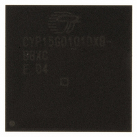
CYP15G0101DXB-BBXC Cypress Semiconductor Corp, CYP15G0101DXB-BBXC Datasheet - Page 6

CYP15G0101DXB-BBXC
Manufacturer Part Number
CYP15G0101DXB-BBXC
Description
IC TXRX HOTLINK 100-LBGA
Manufacturer
Cypress Semiconductor Corp
Series
HOTlink II™r
Type
Transceiverr
Specifications of CYP15G0101DXB-BBXC
Package / Case
100-LBGA
Protocol
Fibre Channel
Voltage - Supply
3.135 V ~ 3.465 V
Mounting Type
Surface Mount
Product
PHY
Data Rate
1500 MBd
Supply Voltage (max)
3.465 V
Supply Voltage (min)
3.135 V
Supply Current
0.5 A
Maximum Operating Temperature
+ 70 C
Minimum Operating Temperature
0 C
Mounting Style
SMD/SMT
Number Of Channels
1
Lead Free Status / RoHS Status
Lead free / RoHS Compliant
For Use With
CYP15G0101DX-EVAL - EVAL BRD FOR HOTLINK II
Number Of Drivers/receivers
-
Lead Free Status / Rohs Status
Lead free / RoHS Compliant
Other names
428-2920
CYP15G0101DXB-BBXC
CYP15G0101DXB-BBXC
Available stocks
Company
Part Number
Manufacturer
Quantity
Price
Company:
Part Number:
CYP15G0101DXB-BBXC
Manufacturer:
MURATA
Quantity:
260 000
Company:
Part Number:
CYP15G0101DXB-BBXC
Manufacturer:
CYPRESS
Quantity:
206
Company:
Part Number:
CYP15G0101DXB-BBXC
Manufacturer:
Cypress Semiconductor Corp
Quantity:
10 000
Part Number:
CYP15G0101DXB-BBXC
Manufacturer:
CYPRESS/赛普拉斯
Quantity:
20 000
Document #: 38-02031 Rev. *J
Pin Descriptions
Pin Name
TXRST
Transmit Path Clock and Clock Control
TXCKSEL
TXCLKO±
TXRATE
TXCLK
Transmit Path Mode Control
TXMODE[1:0] 3-Level Select
Note:
4.
3-Level select inputs are used for static configuration. They are ternary (not binary) inputs that make use of non-standard logic levels of LOW, MID, and HIGH.
The LOW level is usually implemented by direct connection to V
not connected or allowed to float, a 3-Level select input will self-bias to the MID level.
I/O Characteristics Signal Description
LVTTL Input,
asynchronous,
internal pull-up,
sampled by
REFCLK↑
3-Level Select static
control input
LVTTL Output
LVTTL Input,
Static Control input,
internal pull-down
LVTTL Clock Input,
internal pull-down
static control inputs
CYP(V)(W)15G0101DXB Single-channel HOTLink II (continued)
[3]
[4]
[4]
Transmit Clock Phase Reset. Active LOW. When sampled LOW, the transmit Phase-align
Buffer is allowed to adjust its data-transfer timing (relative to the selected input clock) to
allow clean transfer of data from the Input Register to the Encoder or Transmit Shifter. When
TXRST is sampled HIGH, the internal phase relationship between the TXCLK and the
internal character-rate clock is fixed and the device operates normally.
When configured for half-rate REFCLK sampling of the transmit character stream
(TXCKSEL = LOW and TXRATE = HIGH), assertion of TXRST is only used to clear
Phase-align buffer faults caused by highly asymmetric reference clock periods or reference
clocks with excessive cycle-to-cycle jitter. During this alignment period, one or more
characters may be added to or lost from all the associated transmit paths as the transmit
Phase-align Buffers are adjusted. TXRST must be sampled LOW by a minimum of two
consecutive rising edges of REFCLK to ensure the reset operation is initiated correctly on
all channels. This input is ignored when both TXCKSEL and TXRATE are LOW, since the
phase align buffer is bypassed. In all other configurations, TXRST should be asserted during
device initialization to ensure proper operation of the Phase-align buffer. TXRST should be
asserted after the assertion and deassertion of TRSTZ, after the presence of a valid TXCLK
and after allowing enough time for the TXPLL to lock to the reference clock (as specified by
parameter t
Transmit Clock Select. Selects the clock source used to write data into the Transmit Input
Register of the transmit channel. When LOW, the Input Register is clocked by REFCLK↑.
When HIGH or MID, TXCLK↑ is the Input Register clock for TXD[7:0] and TXCT[1:0].
When TXRATE=HIGH, configuring TXCKSEL = HIGH or MID is an invalid mode of
operation.
Transmit Clock Output. This true and complement output clock is synthesized by the
transmit PLL and is synchronous to the internal transmit character clock. It has the same
frequency as REFCLK (when TXRATE = LOW), or twice the frequency of REFCLK (when
TXRATE = HIGH). This output clock has no direct phase relationship to REFCLK.
Transmit PLL Clock Rate Select. When TXRATE = HIGH, the Transmit PLL multiplies
REFCLK by 20 to generate the serial bit-rate clock.
When TXRATE = LOW, the transmit PLL multiplies REFCLK by 10 to generate the serial
bit-rate clock. See Table 9 for a list of operating serial rates.
When REFCLK is selected to clock the receive parallel interfaces (RXCKSEL = LOW), the
TXRATE input also determines if the clocks on the RXCLK± and RXCLKC+ outputs are full
or half-rate. When TXRATE = HIGH (REFCLK is half-rate), the RXCLK± and RXCLKC+
output clocks are also half-rate clocks and follow the frequency and duty cycle of the
REFCLK input. When TXRATE = LOW (REFCLK is full-rate), the RXCLK± and RXCLKC+
output clocks are also full-rate clocks and follow the frequency and duty cycle of the
REFCLK input.
When TXRATE=HIGH, configuring TXCKSEL = HIGH or MID is an invalid mode of
operation.
Transmit Path Input Clock. This clock must be frequency-coherent to TXCLKO±, but may
be offset in phase. The internal operating phase of the input clock (relative to REFLCK or
TXCLKO+) is adjusted when TXRST = LOW and locked when TXRST = HIGH.
Transmit Operating Mode. These inputs are interpreted to select one of nine operating
modes of the transmit path. See Table 3 for a list of operating modes.
TXLOCK
SS
).
(ground). The HIGH level is usually implemented by direct connection to V
CYW15G0101DXB
CYV15G0101DXB
CYP15G0101DXB
CC
Page 6 of 39
(power). When
[3]
[+] Feedback


