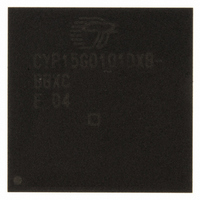
CYP15G0101DXB-BBXC Cypress Semiconductor Corp, CYP15G0101DXB-BBXC Datasheet - Page 8

CYP15G0101DXB-BBXC
Manufacturer Part Number
CYP15G0101DXB-BBXC
Description
IC TXRX HOTLINK 100-LBGA
Manufacturer
Cypress Semiconductor Corp
Series
HOTlink II™r
Type
Transceiverr
Specifications of CYP15G0101DXB-BBXC
Package / Case
100-LBGA
Protocol
Fibre Channel
Voltage - Supply
3.135 V ~ 3.465 V
Mounting Type
Surface Mount
Product
PHY
Data Rate
1500 MBd
Supply Voltage (max)
3.465 V
Supply Voltage (min)
3.135 V
Supply Current
0.5 A
Maximum Operating Temperature
+ 70 C
Minimum Operating Temperature
0 C
Mounting Style
SMD/SMT
Number Of Channels
1
Lead Free Status / RoHS Status
Lead free / RoHS Compliant
For Use With
CYP15G0101DX-EVAL - EVAL BRD FOR HOTLINK II
Number Of Drivers/receivers
-
Lead Free Status / Rohs Status
Lead free / RoHS Compliant
Other names
428-2920
CYP15G0101DXB-BBXC
CYP15G0101DXB-BBXC
Available stocks
Company
Part Number
Manufacturer
Quantity
Price
Company:
Part Number:
CYP15G0101DXB-BBXC
Manufacturer:
MURATA
Quantity:
260 000
Company:
Part Number:
CYP15G0101DXB-BBXC
Manufacturer:
CYPRESS
Quantity:
206
Company:
Part Number:
CYP15G0101DXB-BBXC
Manufacturer:
Cypress Semiconductor Corp
Quantity:
10 000
Part Number:
CYP15G0101DXB-BBXC
Manufacturer:
CYPRESS/赛普拉斯
Quantity:
20 000
Document #: 38-02031 Rev. *J
Pin Descriptions
Pin Name
FRAMCHAR 3-Level Select
RFMODE
PARCTL
DECMODE
RXCKSEL
Device Control Signals
SPDSEL
I/O Characteristics Signal Description
static control input
3-Level Select
static control input
3-Level Select
static control input
3-Level Select
static control input
3-Level Select
static control input
3-Level Select,
static control input
CYP(V)(W)15G0101DXB Single-channel HOTLink II (continued)
[4]
[4]
[4]
[4]
[4]
[4]
Framing Character Select. Used to select the character or portion of a character used for
character framing of the received data streams.
When MID, the Framer looks for both positive and negative disparity versions of the eight-bit
Comma character.
When HIGH, the Framer looks for both positive and negative disparity versions of the K28.5
character.
Configuring FRAMCHAR = LOW is reserved for component test.
Reframe Mode Select. Used to select the type of character framing used to adjust the
character boundaries (based on detection of one or more framing characters in the data
stream. This signal operates in conjunction with the type of framing character selected.
When LOW, the Low-Latency Framer is selected. This will frame on each occurrence of the
selected framing character(s) in the received data stream. This mode of framing stretches
the recovered character-rate clock for one or multiple cycles to align that clock with the
recovered data.
When MID, the Cypress-mode Multi-Byte parallel Framer is selected. This requires a pair
of the selected framing character(s), on identical 10-bit boundaries, within a span of 50 bits
(five characters), before the character boundaries are adjusted. The recovered character
clock remains in the same phase regardless of character offset.
When HIGH, the Alternate-mode Multi-Byte parallel Framer is selected. This requires
detection of the selected framing character(s) in the received data stream, on identical 10-bit
boundaries, on four directly adjacent characters. The recovered character clock remains in
the same phase regardless of character offset.
Parity Check/Generate Control. Used to control the parity check and generate functions.
When LOW, parity checking is disabled, and the RXOP output is disabled (High-Z).
When MID, and the 8B/10B Encoder and Decoder are enabled (TXMODE[1] ≠ LOW,
DECMODE ≠ LOW), TXD[7:0] inputs are checked (along with TXOP) for valid ODD parity,
and ODD parity is generated for the RXD[7:0] outputs and presented on RXOP. When the
8B/10B Encoder and Decoder are disabled (TXMODE[1] = LOW, DECMODE = LOW), the
TXD[7:0] and TXCT[1:0] inputs are checked (along with TXOP) for valid ODD parity, and
ODD parity is generated for the RXD[7:0] and RXST[1:0] outputs and presented on RXOP.
When HIGH, parity generation and checking are enabled. The TXD[7:0] and TXCT[1:0]
inputs are checked (along with TXOP) for valid ODD parity, and ODD parity is generated for
the RXD[7:0] and RXST[2:0] outputs and presented on RXOP.
See Table 2 and Table 15 for details.
Decoder Mode Select. When LOW, the Decoder is bypassed and raw 10-bit characters
are passed to the Output Register. When the Decoder is bypassed, RXCKSEL must be MID.
When MID, the Cypress Decoder table for Special Code Characters is used. When HIGH,
the alternate Decoder table for Special Code Characters is used. See Table 21 for a list of
the Special Codes supported in both encoded modes.
Receive Clock Mode. Selects the receive clock source used to transfer data to the Output
Registers and configures the Elasticity Buffer in the receive path.
When LOW, the Output Register is clocked by REFCLK. RXCLK± and RXCLKC+ present
buffered and delayed forms of REFCLK.
When MID, the RXCLK± output follows the recovered clock as selected by RXRATE and
the Elasticity Buffer is bypassed. When the 10B/8B Decoder and Elasticity Buffer are
bypassed (DECMODE=LOW), RXCKSEL must be MID.
Configuring RXCKSEL = HIGH is an invalid mode of operation.
Serial Rate Select. This input specifies the operating bit-rate range of both transmit and
receive PLLs. LOW = 195–400 MBaud, MID = 400–800 MBaud, HIGH = 800–1500 MBaud
(800–1540 MBaud for CYW15G0101DXB). When SPDSEL=LOW, setting TXRATE=HIGH
(Half-rate Reference Clock) is invalid.
CYW15G0101DXB
CYV15G0101DXB
CYP15G0101DXB
Page 8 of 39
[+] Feedback


