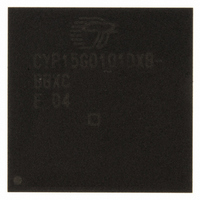
CYP15G0101DXB-BBXC Cypress Semiconductor Corp, CYP15G0101DXB-BBXC Datasheet - Page 7

CYP15G0101DXB-BBXC
Manufacturer Part Number
CYP15G0101DXB-BBXC
Description
IC TXRX HOTLINK 100-LBGA
Manufacturer
Cypress Semiconductor Corp
Series
HOTlink II™r
Type
Transceiverr
Specifications of CYP15G0101DXB-BBXC
Package / Case
100-LBGA
Protocol
Fibre Channel
Voltage - Supply
3.135 V ~ 3.465 V
Mounting Type
Surface Mount
Product
PHY
Data Rate
1500 MBd
Supply Voltage (max)
3.465 V
Supply Voltage (min)
3.135 V
Supply Current
0.5 A
Maximum Operating Temperature
+ 70 C
Minimum Operating Temperature
0 C
Mounting Style
SMD/SMT
Number Of Channels
1
Lead Free Status / RoHS Status
Lead free / RoHS Compliant
For Use With
CYP15G0101DX-EVAL - EVAL BRD FOR HOTLINK II
Number Of Drivers/receivers
-
Lead Free Status / Rohs Status
Lead free / RoHS Compliant
Other names
428-2920
CYP15G0101DXB-BBXC
CYP15G0101DXB-BBXC
Available stocks
Company
Part Number
Manufacturer
Quantity
Price
Company:
Part Number:
CYP15G0101DXB-BBXC
Manufacturer:
MURATA
Quantity:
260 000
Company:
Part Number:
CYP15G0101DXB-BBXC
Manufacturer:
CYPRESS
Quantity:
206
Company:
Part Number:
CYP15G0101DXB-BBXC
Manufacturer:
Cypress Semiconductor Corp
Quantity:
10 000
Part Number:
CYP15G0101DXB-BBXC
Manufacturer:
CYPRESS/赛普拉斯
Quantity:
20 000
Document #: 38-02031 Rev. *J
Pin Descriptions
Pin Name
Receive Path Data Signals
RXD[7:0]
RXST[2:0]
RXOP
Receive Path Clock and Clock Control
RXCLK±
RXCLKC+
RXRATE
RFEN
RXMODE
I/O Characteristics Signal Description
LVTTL Output,
synchronous to the
RXCLK↑ output
(or REFCLK↑ input
when RXCKSEL =
LOW)
LVTTL Output,
synchronous to the
RXCLK↑ output
(or REFCLK↑ input
when RXCKSEL =
LOW)
3-state, LVTTL
Output, synchronous
to the RXCLK↑
output (or REFCLK↑
input
RXCKSEL = LOW)
3-state, LVTTL
Output clock
3-state, LVTTL
Output
LVTTL Input
Static Control Input,
internal pull-down
LVTTL input,
asynchronous,
internal pull-down
3-Level Select
static control input
[3]
CYP(V)(W)15G0101DXB Single-channel HOTLink II (continued)
when
[4]
[3]
[3]
Parallel Data Output. These outputs change following the rising edge of the selected
receive interface clock.
When the Decoder is enabled (DECMODE = HIGH or MID), these outputs represent either
received data or a special character. The status of the received data is represented by the
values of RXST[2:0].
When the Decoder is bypassed (DECMODE = LOW), RXD[7:0] become the higher order
bits of the 10-bit received character. See Table 13 for details.
Parallel Status Output. These outputs change following the rising edge of the selected
receive interface clock.
When the Decoder is bypassed (DECMODE = LOW), RXST[1:0] become the two low-order
bits of the 10-bit received character, while RXST[2] = HIGH indicates the presence of a
Comma character in the Output Register.
When the Decoder is enabled (DECMODE = HIGH or MID), RXST[2:0] provide status of
the received signal. See Table 16 for a list of Receive Character status.
Receive Path Odd Parity. When parity generation is enabled (PARCTL ≠ LOW), the parity
output is valid for the data on the RXD bus bits.
When parity generation is disabled (PARCTL = LOW), this output driver is disabled
(High-Z).
Receive Character Clock Output. When configured such that the output data path is
clocked by the recovered clock (RXCKSEL = MID), these true and complement clocks are
the receive interface clocks which are used to control timing of output data (RXD[7:0],
RXST[2:0] and RXOP). This clock is output continuously at either the dual-character rate
(1/20
received, as selected by RXRATE.
When configured such that the output data path is clocked by REFCLK instead of recovered
clock (RXCKSEL = LOW), the RXCLK± output drivers present a buffered and delayed form
of REFCLK. In this mode, RXCLK± and RXCLKC+ are buffered forms of REFCLK that are
slightly different in phase, but follow the frequency and duty cycle of REFCLK. This phase
difference allows the user to select the optimal set-up/hold timing for their specific interface.
Delayed REFCLK+ when RXCKSEL = LOW. Delayed form of REFCLK+, used for transfer
of output data to a host system. This output is only enabled when the receive parallel
interface is configured to present data relative to REFCLK (RXCKSEL = LOW). When
RXCKSEL = LOW, the RXCLKC+ follows the frequency and duty cycle of REFCLK+.
Receive Clock Rate Select. When LOW, the RXCLK± recovered clock outputs are comple-
mentary clocks operating at the recovered character rate. Data for the receive channel
should be latched on either the rising edge of RXCLK+ or falling edge of RXCLK–.
When HIGH, the RXCLK± recovered clock outputs are complementary clocks operating at
half the character rate. Data for the receive channel should be latched alternately on the
rising edge of RXCLK+ and RXCLK–.
When the output register is operated with REFCLK clocking (RXCKSEL = LOW), RXRATE
is not interpreted and RXCLK± follows the frequency and duty cycle of REFCLK.
Reframe Enable. Active HIGH. When HIGH, the Framer in the receive channel is enabled
to frame per the presently enabled framing mode and selected framing character.
Receive Operating Mode. This input selects one of two RXST channel status reporting
modes and is only interpreted when the Decoder is enabled (DECMODE ≠ LOW). See
Table 12 for details.
th
the serial bit-rate) or character rate (1/10
th
the serial bit-rate) of the data being
CYW15G0101DXB
CYV15G0101DXB
CYP15G0101DXB
Page 7 of 39
[+] Feedback


