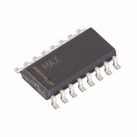
MAX3040CSE+ Maxim Integrated Products, MAX3040CSE+ Datasheet - Page 10

MAX3040CSE+
Manufacturer Part Number
MAX3040CSE+
Description
IC RS485/422 TRANS QUAD 16-SOIC
Manufacturer
Maxim Integrated Products
Type
Transmitterr
Datasheet
1.MAX3045BEUE.pdf
(15 pages)
Specifications of MAX3040CSE+
Number Of Drivers/receivers
4/0
Protocol
RS422, RS485
Voltage - Supply
4.75 V ~ 5.25 V
Mounting Type
Surface Mount
Package / Case
16-SOIC (3.9mm Width)
Data Rate
250 Kbps
Propagation Delay Time Ns
70 ns
Operating Supply Voltage
5 V
Supply Current
1 mA
Operating Temperature Range
0 C to + 70 C
Input Voltage
5 V
Maximum Power Dissipation
696 mW
Mounting Style
SMD/SMT
Output Current
+/- 25 mA to +/- 250 mA
Output Voltage
- 7.5 V to 12.5 V
Product
RS-422/RS-485 Combination
Ic Interface Type
RS422, RS485
No. Of Drivers
4
Supply Voltage Range
4.75V To 5.25V
Driver Case Style
SOIC
No. Of Pins
16
Filter Terminals
SMD
Rohs Compliant
Yes
Data Rate Max
250Kbps
Lead Free Status / RoHS Status
Lead free / RoHS Compliant
required input current. At this time the SR latch resets
and Q1 turns off. When Q1 turns off, EN reverts to a
standard, high-impedance CMOS input. Whenever V
drops below 1V, the hot-swap input is reset.
The EN12 and EN34 input structures are identical to the
EN input. For the EN input, there is a complimentary cir-
cuit employing two PMOS devices pulling the EN input
to V
The circuit of Figure 10 shows a typical offset termina-
tion used to guarantee a greater than 200mV offset
when a line is not driven. The 50pF represents the mini-
mum parasitic capacitance which would exist in a typi-
cal application. In most cases, more capacitance exists
in the system and will reduce the magnitude of the
glitch. During a “hot-swap” event when the driver is
connected to the line and is powered up, the driver
must not cause the differential signal to drop below
200mV. Figures 11 and 12 show the results of the
MAX3040–MAX3045 during power-up for two different
V
the V
the 100Ω termination, the differential signal across the
termination, and shows the hot-swap line transient
stays above the 200mV RS-485 specification.
±10kV ESD-Protected, Quad 5V RS-485/RS-422
Transmitters
10
Figure 9. Simplified Structure of the Driver Enable Pin (EN)
CC
CC
______________________________________________________________________________________
ramp rates (0.1V/µs and 1V/µs). The photos show
CC
.
ramp, the single-ended signal on each side of
Hot-Swap Line Transient
EN
TIMER
5.6kΩ
V
CC
Q1
TIMER
85µA
10µs
CC
700µA
The MAX3040–MAX3045 family has two enable-func-
tional versions:
The MAX3040/MAX3041/MAX3042B have two transmit-
ter enable inputs EN12 and EN34. EN12 controls the
transmitters 1 and 2, and EN34 controls transmitters 3
and 4. EN12 and EN34 are active-high and the part will
enter the low-power shutdown mode when both are
pulled low. The transmitter outputs are high impedance
when disabled (Table 2).
The MAX3043/MAX3044/MAX3045B have two transmit-
ter enable inputs EN and EN, which are active-high and
active-low, respectively. When EN is logic high or EN is
logic low all transmitters are active. When EN is pulled
low and EN is driven high, all transmitters are disabled
and the part enters the low-power shutdown mode. The
transmitter outputs are high impedance when disabled
(Table 3).
The MAX3040–MAX3045 offer optimum performance
when used with the MAX3093E/MAX3095 5V quad
receivers or MAX3094E/MAX3096 3V quad differential
line receivers. Figure 13 shows a typical RS-485 con-
nection for transmitting and receiving data and Figure
14 shows a typical multi-point connection.
Q2
Applications Information
Operation of Enable Pins
(HOT SWAP)
Typical Applications
EN


