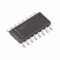
MAX3040CSE+ Maxim Integrated Products, MAX3040CSE+ Datasheet - Page 2

MAX3040CSE+
Manufacturer Part Number
MAX3040CSE+
Description
IC RS485/422 TRANS QUAD 16-SOIC
Manufacturer
Maxim Integrated Products
Type
Transmitterr
Datasheet
1.MAX3045BEUE.pdf
(15 pages)
Specifications of MAX3040CSE+
Number Of Drivers/receivers
4/0
Protocol
RS422, RS485
Voltage - Supply
4.75 V ~ 5.25 V
Mounting Type
Surface Mount
Package / Case
16-SOIC (3.9mm Width)
Data Rate
250 Kbps
Propagation Delay Time Ns
70 ns
Operating Supply Voltage
5 V
Supply Current
1 mA
Operating Temperature Range
0 C to + 70 C
Input Voltage
5 V
Maximum Power Dissipation
696 mW
Mounting Style
SMD/SMT
Output Current
+/- 25 mA to +/- 250 mA
Output Voltage
- 7.5 V to 12.5 V
Product
RS-422/RS-485 Combination
Ic Interface Type
RS422, RS485
No. Of Drivers
4
Supply Voltage Range
4.75V To 5.25V
Driver Case Style
SOIC
No. Of Pins
16
Filter Terminals
SMD
Rohs Compliant
Yes
Data Rate Max
250Kbps
Lead Free Status / RoHS Status
Lead free / RoHS Compliant
ABSOLUTE MAXIMUM RATINGS
All voltages referenced to ground (GND).
Supply Voltage (V
Control Input Voltage (EN,
Driver Input Voltage (T_IN).........................-0.3V to (V
Driver Output Voltage (Y_, Z_)
Driver Output Voltage (Y_, Z_)
Continuous Power Dissipation (T
ELECTRICAL CHARACTERISTICS
(V
±10kV ESD-Protected, Quad 5V RS-485/RS-422
Transmitters
Stresses beyond those listed under “Absolute Maximum Ratings” may cause permanent damage to the device. These are stress ratings only, and functional
operation of the device at these or any other conditions beyond those indicated in the operational sections of the specifications is not implied. Exposure to
absolute maximum rating conditions for extended periods may affect device reliability.
2
DRIVER
Driver Differential Output
Change in Magnitude of
Differential Output Voltage
Driver Common-Mode Output
Voltage
Change In Magnitude of
Common-Mode Voltage
Input High Voltage
Input Low Voltage
Hot-Swap Driver Input Current
Driver Input Current
Driver Short-Circuit Output
Current
Output Leakage (Y_, Z_)
when Disabled
ESD Protection (Y_, Z_)
Electrical Fast Transient/Burst
Immunity
SUPPLY CURRENT
Supply Current
Supply Current in Shutdown
Mode
16-Pin TSSOP (derate 9.4mW/°C above +70°C) ..........755mW
CC
(Driver Disabled) .............................................-7.5V to +12.5V
(Driver Enabled) .................................................-7.5V to +10V
_______________________________________________________________________________________
= +5V ±5%, T
PARAMETER
CC
A
).............................................................+7V
= T
MIN
EN, EN_) .........-0.3V to (V
to T
A
MAX
= +70°C)
SYMBOL
, unless otherwise noted. Typical values are at V
I
∆V
∆V
SWAP
I
SHDN
V
V
V
HOT
I
V
I
I
SC
CC
OD
OC
IN
IH
OD
OC
IL
Figure 1, R = 50Ω
Figure 1, R = 27Ω
Figure 1, R = 50Ω or 27Ω (Note 2)
Figure 1, R = 50Ω or 27Ω
Figure 1, R = 50Ω or 27Ω (Note 2)
T_IN, EN_, EN, EN
T_IN, EN_, EN, EN
EN_, EN, EN (Note 3)
T_IN, EN_, EN, EN
-7V < V OUT < +10V (Note 4)
MAX3040/MAX3041/MAX3042B
EN_ = GND
MAX3043/MAX3044/MAX3045B
EN = GND, EN = V
Human Body Model
IEC 1000-4-4
No load
MAX3040/MAX3041/MAX3042B
EN_ = GND, T
MAX3043/MAX3044/MAX3045B
EN = GND, EN = V
CC
CC
+ 0.3V)
+ 0.3V)
A
CONDITIONS
= +25°C
CC
CC
Operating Temperature Range
Maximum Junction Temperature .....................................+150°C
Storage Temperature Range .............................-65°C to +150°C
Lead Temperature (soldering, 10s) .................................+300°C
, T
16-Pin Narrow SO (derate 8.70mW/°C above +70°C) ..696mW
16-Pin Wide SO (derate 9.52mW/°C above +70°C) .....762mW
MAX304_C_E .......................................................0°C to +70°C
MAX304_E_E ....................................................-40°C to +85°C
A
= +25°C
CC
= +5V and T
MIN
±25
2.0
1.5
2.0
A
= +25°C.) (Note 1)
V
0.002
CC
TYP
±10
±4
1
/ 2
MAX
±200
±250
0.2
0.2
0.8
±1
±1
10
3
2
UNITS
mA
mA
µA
µA
µA
µA
kV
kV
V
V
V
V
V
V


