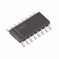
MAX3040CSE+ Maxim Integrated Products, MAX3040CSE+ Datasheet - Page 7

MAX3040CSE+
Manufacturer Part Number
MAX3040CSE+
Description
IC RS485/422 TRANS QUAD 16-SOIC
Manufacturer
Maxim Integrated Products
Type
Transmitterr
Datasheet
1.MAX3045BEUE.pdf
(15 pages)
Specifications of MAX3040CSE+
Number Of Drivers/receivers
4/0
Protocol
RS422, RS485
Voltage - Supply
4.75 V ~ 5.25 V
Mounting Type
Surface Mount
Package / Case
16-SOIC (3.9mm Width)
Data Rate
250 Kbps
Propagation Delay Time Ns
70 ns
Operating Supply Voltage
5 V
Supply Current
1 mA
Operating Temperature Range
0 C to + 70 C
Input Voltage
5 V
Maximum Power Dissipation
696 mW
Mounting Style
SMD/SMT
Output Current
+/- 25 mA to +/- 250 mA
Output Voltage
- 7.5 V to 12.5 V
Product
RS-422/RS-485 Combination
Ic Interface Type
RS422, RS485
No. Of Drivers
4
Supply Voltage Range
4.75V To 5.25V
Driver Case Style
SOIC
No. Of Pins
16
Filter Terminals
SMD
Rohs Compliant
Yes
Data Rate Max
250Kbps
Lead Free Status / RoHS Status
Lead free / RoHS Compliant
The MAX3040–MAX3045 are quad RS-485/RS-422 trans-
mitters. They operate from a single +5V power supply
and are designed to give optimum performance when
used with the MAX3093E/MAX3095 5V quad RS-485/
RS-422 receivers or MAX3094E/MAX3096 3V quad
RS-485/RS-422 receivers. The MAX3040–MAX3045 only
need 1mA of operating supply current and consume 2nA
when they enter a low-power shutdown mode. The
MAX3040–MAX3045 also feature a hot-swap capability
allowing line insertion without erroneous data transfer.
The MAX3042B/MAX3045B are capable of transferring
data up to 20Mbps, the MAX3041/MAX3044 for data
rates up to 2.5Mbps, and the MAX3040/MAX3043 for
data rates up to 250kbps. All transmitter outputs are pro-
tected to ±10kV using the Human Body Model.
As with all Maxim devices, ESD-protection structures
are incorporated on all pins to protect against electro-
static discharges (ESD) encountered during handling
and assembly. The MAX3040–MAX3045 transmitter
outputs have extra protection against electrostatic dis-
charges found in normal operation. Maxim’s engineers
have developed state-of-the-art structures to protect
these pins against the application of ±10kV ESD
(Human Body Model), without damage.
Figure 1. Driver DC Test Circuit
Figure 2. Driver Timing Test Circuit
±10kV ESD-Protected, Quad 5V RS-485/RS-422
Y
Z
DI
DE
5V
_______________________________________________________________________________________
Detailed Description
V
Y
Z
OD
V
OD
±10kV ESD Protection
R
R
R
DIFF
C
V
DIFF
OC
ESD performance depends on a number of conditions.
Contact Maxim for a reliability report that documents
test setup, methodology, and results.
Figure 6a shows the Human Body Model, and Figure
6b shows the current waveform it generates when dis-
charged into low impedance. This model consists of a
100pF capacitor charged to the ESD voltage of interest,
which is then discharged into the device through a
1.5kΩ resistor.
Figure 3. Driver Propagation Delays
Figure 4. Driver Enable/Disable Timing Test Load
Figure 5. Driver Enable and Disable Times
DE
V
Y, Z
Y, Z
V
DIFF
UNDER TEST
3V
OL
DI
0
0
-V
OUTPUT
3V
V
Y
O
O
0
Z
0
1.5V
V
1/2 V
O
1.5V
t
R
10%
O
C
2.5V
2.5V
L
t
t
ZL(SHDN)
ZH(SHDN)
90%
OUTPUT NORMALLY HIGH
OUTPUT NORMALLY LOW
t
PLH
R
L
Transmitters
V
t
SKEW =
DIFF
, t
, t
ZL
ZH
= V (Y) - V (Z)
|
t
PLH
- t
ESD Test Conditions
PHL
Human Body Model
t
t
PHL
t
HZ
LZ
|
t
S1
S2
F
90%
1.5V
1.5V
V
V
OL
OH
V
CC
+0.5V
-0.5V
10%
1/2 V
O
7


