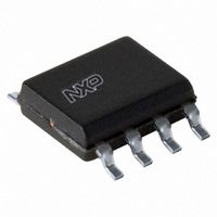
TJA1021T/10/C,118 NXP Semiconductors, TJA1021T/10/C,118 Datasheet - Page 10

TJA1021T/10/C,118
Manufacturer Part Number
TJA1021T/10/C,118
Description
IC TXRX LIN 2.0/SAE J2602 8-SOIC
Manufacturer
NXP Semiconductors
Type
Transceiverr
Datasheet
1.TJA1021TK20C118.pdf
(25 pages)
Specifications of TJA1021T/10/C,118
Package / Case
8-SOIC (3.9mm Width)
Number Of Drivers/receivers
1/1
Protocol
LIN
Voltage - Supply
5.5 V ~ 27 V
Mounting Type
Surface Mount
Mounting Style
SMD/SMT
Lead Free Status / RoHS Status
Lead free / RoHS Compliant
Lead Free Status / RoHS Status
Lead free / RoHS Compliant
Other names
568-4643-2
935285393118
TJA1021T/10/C-T
935285393118
TJA1021T/10/C-T
Available stocks
Company
Part Number
Manufacturer
Quantity
Price
Company:
Part Number:
TJA1021T/10/C,118
Manufacturer:
TI
Quantity:
96
Part Number:
TJA1021T/10/C,118
Manufacturer:
NXP/恩智浦
Quantity:
20 000
NXP Semiconductors
8. Limiting values
Table 5.
In accordance with the Absolute Maximum Rating System (IEC 60134). All voltages are referenced to pin GND; unless
otherwise specified. Positive currents flow into the IC.
[1]
[2]
[3]
[4]
9. Thermal characteristics
Table 6.
According to IEC 60747-1.
TJA1021
Product data sheet
Symbol
V
V
V
V
V
V
I
V
I
V
T
T
Symbol
R
WAKE_N
O(INH)
vj
stg
BAT
TXD
RXD
SLP_N
LIN
WAKE_N
INH
ESD
th(j-a)
Equivalent to discharging a 150 pF capacitor through a 330 resistor; verified by an external test house.
Equivalent to discharging a 100 pF capacitor through a 1.5 k resistor.
Equivalent to discharging a 200 pF capacitor through a 10 resistor and a 0.75 H coil.
Junction temperature in accordance with IEC 60747-1. An alternative definition is: T
The rating for T
Limiting values
Thermal characteristics
Parameter
battery supply voltage
voltage on pin TXD
voltage on pin RXD
voltage on pin SLP_N
voltage on pin LIN
voltage on pin WAKE_N
current on pin WAKE_N
voltage on pin INH
output current on pin INH
electrostatic discharge voltage
virtual junction temperature
storage temperature
Parameter
thermal resistance from junction to ambient
according to IEC 61000-4-2
human body model
charge device model
machine model
vj
limits the allowable combinations of power dissipation (P) and ambient temperature (T
All information provided in this document is subject to legal disclaimers.
Conditions
with respect to GND
I
I
I
I
I
I
with respect to GND, V
current will flow into pin GND
on pins WAKE_N, LIN and V
on pins WAKE_N, LIN, V
on pins RXD, SLP_N and TXD
all pins
all pins
only relevant if V
TXD
TXD
RXD
RXD
SLP_N
SLP_N
no limitation
< 500 A
no limitation
< 500 A
Rev. 7 — 25 March 2011
no limitation
< 500 A
WAKE_N
Conditions
SO8 package; in free air
HVSON8 package; in free air
BAT
< V
BAT
and V
GND
BAT
and INH
0.3
WAKE_N
j
= T
amb
+ P R
LIN 2.1/SAE J2602 transceiver
[1]
[2]
[2]
[3]
[4]
th(j-a)
Min
0.3
0.3
0.3
0.3
0.3
0.3
0.3
40
0.3
15
0.3
50
6
8
2
750
200
40
55
amb
, where R
).
TJA1021
© NXP B.V. 2011. All rights reserved.
Max
+40
+6
+7
+6
+7
+6
+7
+40
+40
-
V
+15
+6
+8
+2
+750
+200
+150
+150
th(j-a)
Typ
145
50
BAT
is a fixed value.
+0.3
Unit
K/W
K/W
10 of 25
Unit
V
V
V
V
V
V
V
V
V
mA
V
mA
kV
kV
kV
V
V
C
C


