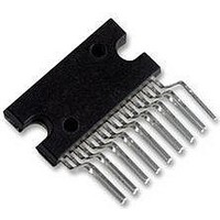
TFA9879HN/N1 NXP Semiconductors, TFA9879HN/N1 Datasheet - Page 23

TFA9879HN/N1
Manufacturer Part Number
TFA9879HN/N1
Description
IC, AMP, AUDIO, MONO, 3W, DBS17P
Manufacturer
NXP Semiconductors
Datasheet
1.TFA9879HNN1118.pdf
(60 pages)
Specifications of TFA9879HN/N1
Amplifier Class
D
No. Of Channels
1
Output Power
2.75W
Load Impedance
8ohm
Operating Temperature Range
-20°C To +85°C
Amplifier Case Style
VQFN
No. Of Pins
24
Base Number
9879
Rohs Compliant
Yes
Supply Voltage Range
2.5V To 5.5V
Thd + N
0.02% @ 100mW, 8ohm, VDD=1.8V
Available stocks
Company
Part Number
Manufacturer
Quantity
Price
Company:
Part Number:
TFA9879HN/N1
Manufacturer:
ALTERA
Quantity:
332
Part Number:
TFA9879HN/N1,118
Manufacturer:
NXP/恩智浦
Quantity:
20 000
NXP Semiconductors
TFA9879
Product data sheet
9.4.1 OverTemperature Protection (OTP)
9.4.2 OverCurrent Protection (OCP)
9.4.3 UnderFrequency Protection (UFP)
The reaction of the device to fault conditions differs depending on the protection circuit
involved.
This is a ‘hard’ protection to prevent heat damage to the TFA9879. Overtemperature
protection is triggered when the junction temperature exceeds 130 °C. When this
happens, the output stages are set floating. OTP can be cleared automatically via a
programmable timer or via the I
operate normally again. The programmable timer settings, selected via bits L_OTP in the
Bypass control register
OTP can also be set to no recovery. Setting the TFA9879 to Off mode and subsequently
to Amplifier mode clears the OTP when no recovery is selected.
The output current of the class-D amplifiers is current limited. When an output stage
exceeds a current in the range 1.3 A to 2.3 A, the output stages are set floating. OCP can
be cleared automatically via a programmable timer or via the I
which the output stages will start to operate normally again. The programmable timer
settings, selected via bits L_OCP in the Bypass control register
The OCP can also be set to no recovery. Setting the TFA9879 to Off mode and
subsequently to Amplifier mode clears the OCP when no recovery is selected.
UFP sets the output stages floating when the clock input source is too low (< f
can happen if, for example, the selected sample frequency (bits I2S_FS in
in line with the applied sample rate. The PWM switching frequency can become critically
low when the frequency of the input clock is lower than the selected sample frequency.
Without UFP, peripheral devices in an application might be damaged.
The UFP status can be monitored by polling the I
will be raised when the input sample rate is too low.
•
•
•
•
•
•
•
•
•
•
•
•
OverTemperature Protection (OTP)
OverCurrent Protection (OCP)
UnderFrequency Protection (UFP)
OverFrequency Protection (OFP)
Invalid Bit-clock Protection (IBP)
DC-blocking via high-pass filter (see
4.5 μs
100 ms
1 s
4.5 μs
27.5 μs
10 ms
All information provided in this document is subject to legal disclaimers.
Rev. 02 — 15 October 2010
(Table
27), are:
2
C-bus interface, after which the output stages will start to
Mono BTL class-D audio amplifier with digital input
Section
2
9.2.3)
C status register
2
C-bus interface, after
(Table
(Table
27), are:
TFA9879
© NXP B.V. 2010. All rights reserved.
Table
33). The alarm
UFP
22) is not
). This
23 of 60


