TFA9879HN/N1 NXP Semiconductors, TFA9879HN/N1 Datasheet - Page 44
TFA9879HN/N1
Manufacturer Part Number
TFA9879HN/N1
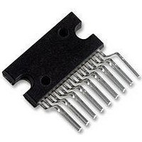
Description
IC, AMP, AUDIO, MONO, 3W, DBS17P
Manufacturer
NXP Semiconductors
Datasheet
1.TFA9879HNN1118.pdf
(60 pages)
Specifications of TFA9879HN/N1
Amplifier Class
D
No. Of Channels
1
Output Power
2.75W
Load Impedance
8ohm
Operating Temperature Range
-20°C To +85°C
Amplifier Case Style
VQFN
No. Of Pins
24
Base Number
9879
Rohs Compliant
Yes
Supply Voltage Range
2.5V To 5.5V
Thd + N
0.02% @ 100mW, 8ohm, VDD=1.8V
Available stocks
Company
Part Number
Manufacturer
Quantity
Price
Company:

Part Number:
TFA9879HN/N1
Manufacturer:
ALTERA
Quantity:
332
Part Number:
TFA9879HN/N1,118
Manufacturer:
NXP/恩智浦
Quantity:
20 000


NXP Semiconductors
15. Application information
TFA9879
Product data sheet
15.1.1 Estimating the RMS output power (P
15.1 Power capability
The TFA9879 is a filter-free BTL class-D amplifier that uses a fixed frequency PWM
modulation scheme (see the simplified application schematic in
TFA9879 is idle (no audio input signal), the voltage across the speaker is 0 V, generating
no additional current. Even when the PWM output is modulated by the audio input signal,
the out-of-band AC ripple current in the voice coil is very small compared to the audio
current. This is due to the inductive behavior of the voice coil at the PWM switching
frequency. A typical voice coil inductance is in the range 30 μH to 80 μH.
The RMS output power, P
using
where:
Example (clip control off):
With V
P
P
The RMS output power at THD + N = 10 % can be estimated using
P
P
P
o(RMS)1%
o(RMS)1%
o RMS
o RMS
0 RMS
Clip control off:
Clip control on:
R
R
R
V
M
(
(
(
DDP
L
S
DSon
max
= load resistance (Ω)
= total series resistance of application
Equation
DDP
)1%
)1%
)10%
= power supply voltage (V)
= maximum modulation depth (clip control on); typically 0.9
= on-resistance of power switch (typically 230 mΩ)
= 1.35 W in an 8
= 2.35 W in a 4
= 5 V, R
=
=
=
⎛
⎝
--------------------------------------------------------------------------------------- -
⎛
⎝
-----------------------------------------------------------------------------------------------------------
1.25
⎛
⎝
⎛
⎝
11, with clip-control off, or using
All information provided in this document is subject to legal disclaimers.
----------------------------------------------------- -
R
----------------------------------------------------- -
R
L
L
+
+
DSon
×
R
R
P
Rev. 02 — 15 October 2010
S
S
0 RMS
(
+
+
= 0.23
R
R
(
(
o(RMS)
2
2
L
L
Ω
2
Ω
)1%
×
×
load
×
R
R
load or
Ω
R
2
DSon
DSon
, at THD + N = 1 % just before clipping can be estimated
L
×
(at T
Mono BTL class-D audio amplifier with digital input
R
)
)
L
⎞
⎠
⎞
⎠
j
×
×
= 25
V
M
DDP
max
o(RMS)
°
C), R
⎞
⎠
×
2
V
Equation
DDP
)
S
= 0.14
⎞
⎠
2
12, with clip-control on.
Ω
:
Figure
Equation
TFA9879
18). When the
© NXP B.V. 2010. All rights reserved.
13:
44 of 60
(12)
(13)
(11)
Related parts for TFA9879HN/N1
Image
Part Number
Description
Manufacturer
Datasheet
Request
R

Part Number:
Description:
The TFA9879 contains a processor that supports a range of sound processing featuresincluding a 5-band parametric equalizer, separate bass and treble control, a dynamicrange compressor, soft clip control and volume control
Manufacturer:
NXP Semiconductors
Datasheet:

Part Number:
Description:
NXP Semiconductors designed the LPC2420/2460 microcontroller around a 16-bit/32-bitARM7TDMI-S CPU core with real-time debug interfaces that include both JTAG andembedded trace
Manufacturer:
NXP Semiconductors
Datasheet:

Part Number:
Description:
NXP Semiconductors designed the LPC2458 microcontroller around a 16-bit/32-bitARM7TDMI-S CPU core with real-time debug interfaces that include both JTAG andembedded trace
Manufacturer:
NXP Semiconductors
Datasheet:
Part Number:
Description:
NXP Semiconductors designed the LPC2468 microcontroller around a 16-bit/32-bitARM7TDMI-S CPU core with real-time debug interfaces that include both JTAG andembedded trace
Manufacturer:
NXP Semiconductors
Datasheet:
Part Number:
Description:
NXP Semiconductors designed the LPC2470 microcontroller, powered by theARM7TDMI-S core, to be a highly integrated microcontroller for a wide range ofapplications that require advanced communications and high quality graphic displays
Manufacturer:
NXP Semiconductors
Datasheet:
Part Number:
Description:
NXP Semiconductors designed the LPC2478 microcontroller, powered by theARM7TDMI-S core, to be a highly integrated microcontroller for a wide range ofapplications that require advanced communications and high quality graphic displays
Manufacturer:
NXP Semiconductors
Datasheet:
Part Number:
Description:
The Philips Semiconductors XA (eXtended Architecture) family of 16-bit single-chip microcontrollers is powerful enough to easily handle the requirements of high performance embedded applications, yet inexpensive enough to compete in the market for hi
Manufacturer:
NXP Semiconductors
Datasheet:
Part Number:
Description:
The XA-S3 device is a member of Philips Semiconductors? XA(eXtended Architecture) family of high performance 16-bitsingle-chip microcontrollers
Manufacturer:
NXP Semiconductors
Datasheet:

Part Number:
Description:
The NXP BlueStreak LH75401/LH75411 family consists of two low-cost 16/32-bit System-on-Chip (SoC) devices
Manufacturer:
NXP Semiconductors
Datasheet:
Part Number:
Description:
The NXP LPC3130/3131 combine an 180 MHz ARM926EJ-S CPU core, high-speed USB2
Manufacturer:
NXP Semiconductors
Datasheet:
Part Number:
Description:
The NXP LPC3141 combine a 270 MHz ARM926EJ-S CPU core, High-speed USB 2
Manufacturer:
NXP Semiconductors
Part Number:
Description:
The NXP LPC3143 combine a 270 MHz ARM926EJ-S CPU core, High-speed USB 2
Manufacturer:
NXP Semiconductors

Part Number:
Description:
The NXP LPC3152 combines an 180 MHz ARM926EJ-S CPU core, High-speed USB 2
Manufacturer:
NXP Semiconductors
Part Number:
Description:
The NXP LPC3154 combines an 180 MHz ARM926EJ-S CPU core, High-speed USB 2
Manufacturer:
NXP Semiconductors