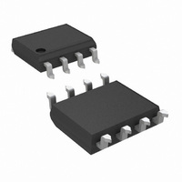
CLC001AJE-TR13/NOPB National Semiconductor, CLC001AJE-TR13/NOPB Datasheet - Page 10

CLC001AJE-TR13/NOPB
Manufacturer Part Number
CLC001AJE-TR13/NOPB
Description
IC CABLE DRIVER DGTL ADJ 8-SOIC
Manufacturer
National Semiconductor
Series
CLCr
Type
Driverr
Datasheet
1.CLC001AJENOPB.pdf
(11 pages)
Specifications of CLC001AJE-TR13/NOPB
Number Of Drivers/receivers
1/0
Protocol
LVDS
Voltage - Supply
3 V ~ 3.6 V
Mounting Type
Surface Mount
Package / Case
8-SOIC (3.9mm Width)
For Use With
SD001EVK - BOARD EVALUATION CLC001DRIVECABLE02EVK - BOARD EVAL SERDES, CLC001, 012
Lead Free Status / RoHS Status
Lead free / RoHS Compliant
Other names
CLC001AJE-TR13
CLC001AJETR
CLC001AJETR
Available stocks
Company
Part Number
Manufacturer
Quantity
Price
Company:
Part Number:
CLC001AJE-TR13/NOPB
Manufacturer:
NXP
Quantity:
4 265
Part Number:
CLC001AJE-TR13/NOPB
Manufacturer:
TI/德州仪器
Quantity:
20 000
www.national.com
Device Operation
OUTPUT INTERFACING
The CLC001 has two complementary, ground referenced
outputs designed to drive AC-coupled and terminated 75Ω
coaxial cables. The outputs are single ended; however, they
could be treated as a single differential output as long as
current paths from each output go to ground.
The output of the CLC001 is a high impedance current
source. It expects to see a 75Ω shunt resistor before driving
cable to convert the current output to a voltage and provide
proper back-matching. No series back-matching resistors
should be used. Refer to Section Typical Application for an
illustration.
Output levels range from 800 mV
75Ω AC-coupled, back-matched loads. Output level is con-
trolled by the value of R
kΩ
to Figure 10 for the output level’s sensitivity to R
Evaluation Board
Evaluation boards are available for a nominal charge that
demonstrate the basic operation of the SDI/SDV/SDH de-
±
1% for 800 mV
FIGURE 10. Output level’s sensitivity to R
p-p
, and 1.5 kΩ
REF
connected to pin 4. R
(Continued)
p-p
±
to 1.0 V
1% for 1.0 V
10132913
p-p
REF
REF
±
p-p
REF
10% into
.
. Refer
is 1.91
10
vices. The evaluation boards can be ordered through Nation-
al’s Distributors. Supplies are limited, please check for cur-
rent availability.
The SD001EVK evaluation kit for the CLC001, Serial Digital
Cable Driver with Adjustable Outputs, provides an operating
environment in which the cable driver can be evaluated by
system / hardware designers. The evaluation board has all
the needed circuitry and connectors for easy connection and
checkout of the device circuit options as discussed in the
CLC001 datasheet. A schematic, parts list and pictorial
drawing are provided with the board.
From the WWW, the following information may be viewed /
downloaded for most evaluation boards: www.national.com/
appinfo/interface
• Device Datasheet and / or EVK User Manual
• View a picture of the EVK
• View the EVK Schematic
• View the top assembly drawing and BOM
• View the bottom assembly drawing and BOM
PCB Layout Recommendations
Printed circuit board layout affects the performance of the
CLC001. The following guidelines will aid in achieving satis-
factory device performance.
• Use a ground plane or power/ground plane sandwich
• Bypass device power with a 0.01 µF monolithic ceramic
• Provide short, symmetrical ground return paths for:
• Provide short, grounded guard traces located
design for optimum performance.
capacitor in parallel with a 6.8 µF tantalum electrolytic
capacitor located no more than 0.1" (2.5 mm) from the
device power pins.
— inputs,
— supply bypass capacitors and
— the output load.
— under the centerline of the package,
— 0.1" (2.5 mm) from the package pins
— on both top and bottom of the board with connecting
vias.


