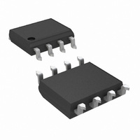
CLC001AJE-TR13/NOPB National Semiconductor, CLC001AJE-TR13/NOPB Datasheet - Page 4

CLC001AJE-TR13/NOPB
Manufacturer Part Number
CLC001AJE-TR13/NOPB
Description
IC CABLE DRIVER DGTL ADJ 8-SOIC
Manufacturer
National Semiconductor
Series
CLCr
Type
Driverr
Datasheet
1.CLC001AJENOPB.pdf
(11 pages)
Specifications of CLC001AJE-TR13/NOPB
Number Of Drivers/receivers
1/0
Protocol
LVDS
Voltage - Supply
3 V ~ 3.6 V
Mounting Type
Surface Mount
Package / Case
8-SOIC (3.9mm Width)
For Use With
SD001EVK - BOARD EVALUATION CLC001DRIVECABLE02EVK - BOARD EVAL SERDES, CLC001, 012
Lead Free Status / RoHS Status
Lead free / RoHS Compliant
Other names
CLC001AJE-TR13
CLC001AJETR
CLC001AJETR
Available stocks
Company
Part Number
Manufacturer
Quantity
Price
Company:
Part Number:
CLC001AJE-TR13/NOPB
Manufacturer:
NXP
Quantity:
4 265
Part Number:
CLC001AJE-TR13/NOPB
Manufacturer:
TI/德州仪器
Quantity:
20 000
www.national.com
t
t
t
t
r
os
jit
pd
Symbol
, t
AC Electrical Characteristics
Over recommended operating supply and temperature ranges unless otherwise specified (Note 3)
Note 1: “Absolute Maximum Ratings” are those values beyond which the safety of the device cannot be guaranteed. They are not meant to imply that the devices
should be operated at these limits. The table of “Electrical Characteristics” specifies conditions of device operation.
Note 2: Current flow into device pins is defined as positive. Current flow out of device pins is defined as negative. All voltages are stated referenced to V
Note 3: Typical values are at 25˚C and 3.3V.
Note 4: This parameter is Guaranteed by Design.
Note 5: R
Note 6: The V
power other devices.
Note 7: R
Note 8: Input Current Balance (I
Test Loads
f
L
L
= 75Ω, AC-coupled at 270 Mbps, R
= 75Ω, AC-coupled at 622 Mbps, R
Rise time, Fall time
Output overshoot
Output jitter
Propagation delay
BB
output is intended as a bias supply pin for the inputs of this device only. It is not designed as a power supply output and should not be used to
Parameter
INB
) is the difference between the Input Current (I
REF
REF
= 1.91 kΩ 1% (for V
= 1.5 kΩ 1% (for V
20%–80%, (Notes 4, 5)
(Note 7)
(Note 5)
FIGURE 1. Test Loads
SDO
SDO
= 1.0 V
= 800 mV
4
IN
Conditions
p-p
) on V
±
p-p
10%), clock pattern input.
±
IN+
10%), C
and V
L
IN−
not greater than 5pF (See Figure 1)
for the same bias condition.
Min
10132904
Typ
400
1.9
25
5
Max
800
SS
Units
= 0V.
ps
ps
ns
%


