DS90CF386MTDX/NOPB National Semiconductor, DS90CF386MTDX/NOPB Datasheet - Page 11
DS90CF386MTDX/NOPB
Manufacturer Part Number
DS90CF386MTDX/NOPB
Description
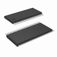
IC RVR LVDS FPD 3.3V 56-TSSOP
Manufacturer
National Semiconductor
Type
Receiverr
Datasheet
1.DS90CF386MTDNOPB.pdf
(18 pages)
Specifications of DS90CF386MTDX/NOPB
Number Of Drivers/receivers
0/1
Protocol
RS644
Voltage - Supply
3 V ~ 3.6 V
Mounting Type
Surface Mount
Package / Case
56-TSSOP
For Use With
FLINK3V8BT-85 - BOARD EVAL DS90C385A,DS90CF386
Lead Free Status / RoHS Status
Lead free / RoHS Compliant
Other names
*DS90CF386MTDX
DS90CF386MTDX
DS90CF386MTDX
Available stocks
Company
Part Number
Manufacturer
Quantity
Price
Company:

Part Number:
DS90CF386MTDX/NOPB
Manufacturer:
TI
Quantity:
3 132
Part Number:
DS90CF386MTDX/NOPB
Manufacturer:
TI/德州仪器
Quantity:
20 000


RxIN+
RxIN−
RxOUT
RxCLK IN+
RxCLK IN−
RxCLK OUT
PWR DOWN
V
GND
PLL V
PLL GND
LVDS V
LVDS GND
RxIN+
RxIN−
RxOUT
RxCLK IN+
RxCLK IN−
RxCLK OUT
PWR DOWN
V
GND
PLL V
PLL GND
LVDS V
LVDS GND
RxIN+
RxIN−
RxOUT
RxCLK IN+
RxCLK IN−
FPSHIFT OUT
PWR DOWN
V
GND
CC
CC
CC
DS90CF386 MTD56 Package Pin Descriptions—24-Bit FPD Link Receiver
DS90CF366 MTD48 Package Pin Descriptions—18-Bit FPD Link Receiver
DS90CF386 — 64 ball FBGA package Pin Descriptions —
FPD Link Receiver
Pin Name
Pin Name
Pin Name
CC
CC
CC
CC
I/O No
I/O No
I/O No
O
O
O
O
O
O
I
I
I
I
I
I
I
I
I
I
I
I
I
I
I
I
I
I
I
I
I
I
I
I
I
I
I
I
I
21 TTL level data outputs. This includes: 6 Red, 6 Green, 6 Blue, and 3 control lines—FPLINE, FPFRAME,
28 TTL level data outputs. This includes: 8 Red, 8 Green, 8 Blue, and 4 control lines—FPLINE, FPFRAME,
28 TTL level data outputs. This includes: 8 Red, 8 Green, 8 Blue, and 3 control lines—FPLINE, FPFRAME,
3 Positive LVDS differentiaI data inputs.
3 Negative LVDS differential data inputs.
1 Positive LVDS differential clock input.
1 Negative LVDS differential clock input.
1 TTL Ievel clock output. The falling edge acts as data strobe.
1 TTL level input. When asserted (low input) the receiver outputs are low.
4 Power supply pins for TTL outputs.
5 Ground pins for TTL outputs.
1 Power supply for PLL.
2 Ground pin for PLL.
1 Power supply pin for LVDS inputs.
3 Ground pins for LVDS inputs.
4 Positive LVDS differentiaI data inputs.
4 Negative LVDS differential data inputs.
1 Positive LVDS differential clock input.
1 Negative LVDS differential clock input.
1 TTL Ievel clock output. The falling edge acts as data strobe. Pin name RxCLK OUT.
1 TTL level input. When asserted (low input) the receiver outputs are low.
4 Power supply pins for TTL outputs.
5 Ground pins for TTL outputs.
4
4
1
1
1
1
4
5
1
2
1
3
.
.
.
DRDY (also referred to as HSYNC, VSYNC, Data Enable).
DRDY (also referred to as HSYNC, VSYNC, Data Enable).
Positive LVDS differentiaI data inputs.
Negative LVDS differential data inputs.
DRDY (also referred to as HSYNC, VSYNC, Data Enable).
Positive LVDS differential clock input.
Negative LVDS differential clock input.
TTL Ievel clock output. The falling edge acts as data strobe.
TTL level input. When asserted (low input) the receiver outputs are low.
Power supply pins for TTL outputs.
Ground pins for TTL outputs.
Power supply for PLL.
Ground pin for PLL.
Power supply pin for LVDS inputs.
Ground pins for LVDS inputs.
11
Description
Description
Description
www.national.com
Related parts for DS90CF386MTDX/NOPB
Image
Part Number
Description
Manufacturer
Datasheet
Request
R

Part Number:
Description:
National Semiconductor [8-Bit D/A Converter]
Manufacturer:
National Semiconductor
Datasheet:
Part Number:
Description:
National Semiconductor [Media Coprocessor]
Manufacturer:
National Semiconductor
Datasheet:
Part Number:
Description:
Digitally Controlled Tone and Volume Circuit with Stereo Audio Power Amplifier, Microphone Preamp Stage and National 3D Sound
Manufacturer:
National Semiconductor
Datasheet:
Part Number:
Description:
Digitally Controlled Tone and Volume Circuit with Stereo Audio Power Amplifier, Microphone Preamp Stage and National 3D Sound
Manufacturer:
National Semiconductor
Datasheet:
Part Number:
Description:
AC97 Rev 2 Codec with Sample Rate Conversion and National 3D Sound
Manufacturer:
National Semiconductor
Part Number:
Description:
Manufacturer:
National Semiconductor
Datasheet:
Part Number:
Description:
Manufacturer:
National Semiconductor
Datasheet:
Part Number:
Description:
General Purpose, Low Voltage, Low Power, Rail-to-Rail Output Operational Amplifiers
Manufacturer:
National Semiconductor
Datasheet:
Part Number:
Description:
8-bit 20 MSPS flash A/D converter.
Manufacturer:
National Semiconductor
Datasheet:
Part Number:
Description:
Low Noise Quad Operational Amplifier
Manufacturer:
National Semiconductor
Datasheet:
Part Number:
Description:
Quad Differential Line Receivers
Manufacturer:
National Semiconductor
Datasheet:
Part Number:
Description:
Quad High Speed Trapezoidal? Bus Transceiver
Manufacturer:
National Semiconductor
Datasheet:
Part Number:
Description:
Dual Line Receiver
Manufacturer:
National Semiconductor
Datasheet:
Part Number:
Description:
TTL to 10k ECL Level Translator with Latch
Manufacturer:
National Semiconductor
Datasheet: