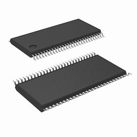
DS90CF386MTDX/NOPB National Semiconductor, DS90CF386MTDX/NOPB Datasheet - Page 3

DS90CF386MTDX/NOPB
Manufacturer Part Number
DS90CF386MTDX/NOPB
Description
IC RVR LVDS FPD 3.3V 56-TSSOP
Manufacturer
National Semiconductor
Type
Receiverr
Datasheet
1.DS90CF386MTDNOPB.pdf
(18 pages)
Specifications of DS90CF386MTDX/NOPB
Number Of Drivers/receivers
0/1
Protocol
RS644
Voltage - Supply
3 V ~ 3.6 V
Mounting Type
Surface Mount
Package / Case
56-TSSOP
For Use With
FLINK3V8BT-85 - BOARD EVAL DS90C385A,DS90CF386
Lead Free Status / RoHS Status
Lead free / RoHS Compliant
Other names
*DS90CF386MTDX
DS90CF386MTDX
DS90CF386MTDX
Available stocks
Company
Part Number
Manufacturer
Quantity
Price
Company:
Part Number:
DS90CF386MTDX/NOPB
Manufacturer:
TI
Quantity:
3 132
Part Number:
DS90CF386MTDX/NOPB
Manufacturer:
TI/德州仪器
Quantity:
20 000
ICCRZ
CLHT
CHLT
RSPos0
RSPos1
RSPos2
RSPos3
RSPos4
RSPos5
RSPos6
RSKM
RCOP
RCOH
RCOL
RSRC
RHRC
RCCD
RPLLS
RPDD
Symbol
Symbol
Note 1: “Absolute Maximum Ratings” are those values beyond which the safety of the device cannot be guaranteed. They are not meant to imply that the device
should be operated at these limits. The tables of “Electrical Characteristics” specify conditions for device operation.
Note 2: Typical values are given for V
Note 3: Current into device pins is defined as positive. Current out of device pins is defined as negative. Voltages are referenced to ground unless otherwise
specified (except V
Receiver Switching Characteristics
Over recommended operating supply and temperature ranges unless otherwise specified
Note 4: Receiver Skew Margin is defined as the valid data sampling region at the receiver inputs. This margin takes into account the transmitter pulse positions
(min and max) and the receiver input setup and hold time (internal data sampling window - RSPos). This margin allows for LVDS interconnect skew, inter-symbol
interference (both dependent on type/length of cable), and clock jitter (less than 150 ps).
Receiver Supply Current
Power Down
CMOS/TTL Low-to-High Transition Time
CMOS/TTL High-to-Low Transition Time
Receiver Input Strobe Position for Bit 0
Figure 12
Receiver Input Strobe Position for Bit 1
Receiver Input Strobe Position for Bit 2
Receiver Input Strobe Position for Bit 3
Receiver Input Strobe Position for Bit 4
Receiver Input Strobe Position for Bit 5
Receiver Input Strobe Position for Bit 6
RxIN Skew Margin
RxCLK OUT Period
RxCLK OUT High Time
RxCLK OUT Low Time
RxOUT Setup to RxCLK OUT
RxOUT Hold to RxCLK OUT
RxCLK IN to RxCLK OUT Delay @ 25°C, V
Receiver Phase Lock Loop Set
Receiver Power Down Delay
OD
and ΔV
)
Parameter
OD
).
(Note
CC
(Figure
= 3.3V and T
(Figure
(Figure 5
4)
5)
(Figure 13
(Figure 5
(Figure 10
(Figure 5
Parameter
5)
(Figure 7
A
)
= +25C.
)
)
)
(Figure
)
)
(Figures 2, 3, 4 )
Power Down = Low
Receiver Outputs Stay Low during
Power Down Mode
(Figure 4
(Figure 4
CC
= 3.3V
11,
)
)
3
(Figure 6
f = 85 MHz
f = 85 MHz
f = 85 MHz
Conditions
)
f = 65 MHz
f = 85 MHz
10.57
11.76
0.49
2.17
3.85
5.53
7.21
8.89
Min
290
4.5
4.0
2.0
3.5
5.5
Min
10.92
0.84
2.52
4.20
5.88
7.56
9.24
Typ
2.0
1.8
7.0
T
5
5
Typ
140
43
43
11.27
Max
1.19
2.87
4.55
6.23
7.91
9.59
3.5
3.5
6.5
9.5
50
10
7
1
Max
400
60
70
www.national.com
Units
Units
mA
mA
μA
ms
ns
ns
ns
ns
ns
ns
ns
ns
ns
ps
ns
ns
ns
ns
ns
ns
μs


