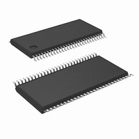
DS90CF386MTDX/NOPB National Semiconductor, DS90CF386MTDX/NOPB Datasheet - Page 2

DS90CF386MTDX/NOPB
Manufacturer Part Number
DS90CF386MTDX/NOPB
Description
IC RVR LVDS FPD 3.3V 56-TSSOP
Manufacturer
National Semiconductor
Type
Receiverr
Datasheet
1.DS90CF386MTDNOPB.pdf
(18 pages)
Specifications of DS90CF386MTDX/NOPB
Number Of Drivers/receivers
0/1
Protocol
RS644
Voltage - Supply
3 V ~ 3.6 V
Mounting Type
Surface Mount
Package / Case
56-TSSOP
For Use With
FLINK3V8BT-85 - BOARD EVAL DS90C385A,DS90CF386
Lead Free Status / RoHS Status
Lead free / RoHS Compliant
Other names
*DS90CF386MTDX
DS90CF386MTDX
DS90CF386MTDX
Available stocks
Company
Part Number
Manufacturer
Quantity
Price
Company:
Part Number:
DS90CF386MTDX/NOPB
Manufacturer:
TI
Quantity:
3 132
Part Number:
DS90CF386MTDX/NOPB
Manufacturer:
TI/德州仪器
Quantity:
20 000
www.national.com
CMOS/TTL DC SPECIFICATIONS
V
V
V
V
V
I
I
LVDS RECEIVER DC SPECIFICATIONS
V
V
I
RECEIVER SUPPLY CURRENT
ICCRW
ICCRW
ICCRG
IN
OS
Symbol
IN
IH
IL
OH
OL
CL
TH
TL
Absolute Maximum Ratings
If Military/Aerospace specified devices are required,
please contact the National Semiconductor Sales Office/
Distributors for availability and specifications.
Supply Voltage (V
CMOS/TTL Output Voltage
LVDS Receiver Input Voltage
Junction Temperature
Storage Temperature
Lead Temperature
Solder Reflow Temperature
Maximum Package Power
Dissipation Capacity @ 25°C
Package Derating:
Electrical Characteristics
Over recommended operating supply and temperature ranges unless otherwise specified.
TSSOP)
MTD56 (TSSOP) Package:
MTD48 (TSSOP) Package:
DS90CF386MTD
(Soldering, 4 sec for
(Soldering, 20 sec for FBGA)
DS90CF386MTD
DS90CF366MTD
High Level Input Voltage
Low Level Input Voltage
High Level Output Voltage
Low Level Output Voltage
Input Clamp Voltage
Input Current
Output Short Circuit Current
Differential Input High Threshold
Differential Input Low Threshold
Input Current
Receiver Supply Current
Worst Case
Receiver Supply Current
Worst Case
Receiver Supply Current,
16 Grayscale
CC
)
Parameter
12.4 mW/°C above +25°C
−0.3V to (V
−0.3V to (V
−65°C to +150°C
−0.3V to +4V
(Note
CC
CC
I
I
I
V
V
V
V
V
V
C
Worst Case Pattern,
DS90CF386 (Figures 1,
4 )
C
Worst Case Pattern,
DS90CF366 (Figures 1,
4 )
C
16 Grayscale Pattern,
OH
OL
CL
+150°C
+260°C
+220°C
+ 0.3V)
+ 0.3V)
1.61 W
1.89 W
IN
IN
OUT
L
L
L
1)
CM
IN
IN
= 8 pF,
= 8 pF,
= 8 pF,
= 2 mA
= −18 mA
= - 0.4 mA
= 0.4V, 2.5V or V
= GND
= +2.4V, V
= 0V, V
= +1.2V
= 0V
CC
2
= 3.6V
CC
Maximum Package Power
Dissipation Capacity @ 25°C
Package Derating:
ESD Rating
Recommended Operating
Conditions
Conditions
= 3.6V
DS90CF366MTD
SLC64A Package:
DS90CF386SLC
(HBM, 1.5 kΩ, 100 pF)
Supply Voltage (V
Operating Free Air
Receiver Input Range
Supply Noise Voltage (V
DS90CF386SLC
(EIAJ, 0Ω, 200 pF)
CC
Temperature (T
f = 32.5 MHz
f = 37.5 MHz
f = 65 MHz
f = 85 MHz
f = 32.5 MHz
f = 37.5 MHz
f = 65 MHz
f = 85 MHz
f = 32.5 MHz
f = 37.5 MHz
CC
A
)
)
CC
)
GND
−100
Min
2.0
2.7
-10
Min
−10 +25 +70
3.0
10.2 mW/°C above +25°C
0
15 mW/°C above +25°C
-0.79
0.06
+1.8
Typ
3.3
No
3.3
-60
m
49
53
81
96
49
53
78
90
28
30
0
Max Units
100
3.6
2.4
+100
VCC
-120
Max
-1.5
+15
±10
±10
114
135
100
115
0.8
0.3
70
75
60
65
45
47
mV
°C
> 700V
V
V
> 7 kV
2.0 W
PP
Units
mA
mV
mV
mA
mA
mA
mA
mA
mA
mA
mA
mA
mA
uA
uA
μA
μA
V
V
V
V
V


