MC74LVX4245DTG ON Semiconductor, MC74LVX4245DTG Datasheet
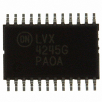
IC TXRX DUAL OCT 3ST LV 24TSSOP

MC74LVX4245DTG

Manufacturer Part Number
MC74LVX4245DTG
Description
IC TXRX DUAL OCT 3ST LV 24TSSOP
Manufacturer
ON Semiconductor
Series
LVXr
Type
Transceiverr
Datasheet

Specifications of MC74LVX4245DTG

Number Of Drivers/receivers
8/8
Voltage - Supply
2.7 V ~ 5.5 V
Mounting Type
Surface Mount
Package / Case
24-TSSOP
Logic Type
CMOS
Logic Family
74LVX
Number Of Channels Per Chip
8
Input Level
CMOS
Output Level
CMOS
Output Type
3-State
High Level Output Current
- 24 mA
Low Level Output Current
24 mA
Propagation Delay Time
10 ns
Supply Voltage (max)
3.6 V, 5.5 V
Supply Voltage (min)
2.7 V, 4.5 V
Maximum Operating Temperature
+ 85 C
Function
Bus Transceiver with Voltage Translation
Input Bias Current (max)
8 uA
Maximum Power Dissipation
200 mW
Minimum Operating Temperature
- 40 C
Mounting Style
SMD/SMT
Number Of Circuits
2
Polarity
Non-Inverting
Operating Supply Voltage (typ)
3.3/5V
Number Of Elements
1
Number Of Channels
8
Input Logic Level
CMOS
Output Logic Level
CMOS
Package Type
TSSOP
Logical Function
Bus Transceiver with Voltage Translation
Operating Supply Voltage (min)
2.7/4.5V
Technology
CMOS
Operating Temp Range
-40C to 85C
Operating Temperature Classification
Industrial
Mounting
Surface Mount
Additional Features
W/Volt Translation
Pin Count
24
Lead Free Status / RoHS Status
Lead free / RoHS Compliant
Protocol
-
Lead Free Status / Rohs Status
Lead free / RoHS Compliant
Other names
MC74LVX4245DTGOS
MC74LVX4245
Dual Supply Octal
Translating Transceiver
with 3−State Outputs
transceiver that is designed to interface between a 5.0 V bus and a 3.0 V
bus in a mixed 3.0 V / 5.0 V supply environment such as laptop
computers using a 3.3 V CPU and 5.0 V LCD display. The A port
interfaces with the 5V bus; the B port interfaces with the 3.0 V bus.
flow. Transmit (active−High) enables data from the A port to the B
port. Receive (active−Low) enables data from the B port to the A port.
The Output Enable (OE) input, when High, disables both A and B
ports by placing them in 3−State.
Features
*For additional information on our Pb−Free strategy and soldering details, please
March, 2005 − Rev. 4
download the ON Semiconductor Soldering and Mounting Techniques
Reference Manual, SOLDERRM/D.
V
The 74LVX4245 is a 24−pin dual−supply, octal translating
The Transmit/Receive (T/R) input determines the direction of data
V
Threshold Performance
Bi−directional Interface Between 5.0 V and 3.0 V Buses
Control Inputs Compatible with TTL Level
5.0 V Data Flow at A Port and 3.0 V Data Flow at B Port
Outputs Source/Sink 24 mA at 5.0 V Bus and 12 mA at 3.0 V Bus
Guaranteed Simultaneous Switching Noise Level and Dynamic
Available in SOIC and TSSOP Packages
Functionally Compatible with the 74 Series 245
Pb−Free Packages are Available*
Semiconductor Components Industries, LLC, 2005
CCB
24
CCA
1
V
T/R
23
CCB
2
OE
22
A0
3
B0
21
A1
Figure 1. 24−Lead Pinout
4
B1
20
A2
5
(Top View)
B2
19
A3
6
B3
18
A4
7
B4
A5
17
8
B5
A6
16
9
B6
15
10
A7
GND GND
B7
14
11
GND
13
12
1
24
See detailed ordering and shipping information in the package
dimensions section on page 5 of this data sheet.
PIN NAMES
Pins
OE
T/R
A0−A7
B0−B7
24
1
1
ORDERING INFORMATION
A
WL
YY
WW
Function
Output Enable Input
Transmit/Receive Input
Side A 3−State Inputs or 3−State
Outputs
Side B 3−State Inputs or 3−State
Outputs
http://onsemi.com
DW SUFFIX
CASE 751E
CASE 948H
DT SUFFIX
TSSOP−24
SOIC−24
= Assembly Location
= Wafer Lot
= Year
= Work Week
Publication Order Number:
24
1
24
1
DIAGRAMS
MC74LVX4245/D
MARKING
AWLYYWW
AWLYYWW
LVXC4245
4245
LVX

Related parts for MC74LVX4245DTG

MC74LVX4245DTG Summary of contents

Page 1

... V T CCA Figure 1. 24−Lead Pinout (Top View) *For additional information on our Pb−Free strategy and soldering details, please download the ON Semiconductor Soldering and Mounting Techniques Reference Manual, SOLDERRM/D. Semiconductor Components Industries, LLC, 2005 March, 2005 − Rev GND GND GND 1 http://onsemi.com ...

Page 2

MC74LVX4245 Figure 2. Logic Diagram INPUTS OE T High Voltage Level; L ...

Page 3

ABSOLUTE MAXIMUM RATINGS Symbol Parameter Supply Voltage CCA V CCB V DC Input Voltage Input/Output Voltage I Input Diode Current Output Diode Current Output Source/Sink Current ...

Page 4

DC ELECTRICAL CHARACTERISTICS Symbol Parameter I Max Input Leak- IN OE, age T/R Current I Max 3−State Out- OZA put Leakage An I Max 3−State Out- OZB put Leakage Bn DI Maximum I An,OE CC CCT T/R per Input Bn ...

Page 5

AC ELECTRICAL CHARACTERISTICS Symbol Parameter t Propagation Delay PHL t PLH t Propagation Delay PHL t PLH t Output Enable Time PZL t PZH t Output Enable Time ...

Page 6

Dual Supply Octal Translating Transceiver The 74LVX4245 dual−supply device well capable of bidirectional signal voltage translation. This level shifting ability provides an excellent interface between low voltage CPU local bus and a standard 5.0 V I/O ...

Page 7

MC74LVX4245 MICROCHANNEL/ EISA/ISA/ BUS KEYBOARD CONTROLLER SUPER 5V I/O V CCA CORE LOGIC A PORT TRANSCEIVERS A0:7 PCMCIA CONTROLLER VGA CONTROLLER Figure 4. MC74LVX4245 Fits Into a System with 3V Subsystem and 5V Subsystem V CCA (T/R) DIR ...

Page 8

MC74LVX4245 50 PLH Bn, An WAVEFORM 1 − PROPAGATION DELAYS 2.5ns, 10 1MHz 50% V OE, T PZH An PZL ...

Page 9

D 24X 0.010 (0.25 −T− SEATING PLANE G 22X MC74LVX4245 PACKAGE DIMENSIONS SOIC−24 DW SUFFIX CASE 751E−04 ISSUE E 13 −B− P 12X 0.010 (0.25 ...

Page 10

... DETAIL DETAIL E N. American Technical Support: 800−282−9855 Toll Free USA/Canada Japan: ON Semiconductor, Japan Customer Focus Center 2−9−1 Kamimeguro, Meguro−ku, Tokyo, Japan 153−0051 Phone: 81−3−5773−3850 http://onsemi.com 10 NOTES: 1. DIMENSIONING AND TOLERANCING PER ANSI Y14 ...

Related keywords