MC74LVX4245DTG ON Semiconductor, MC74LVX4245DTG Datasheet - Page 4
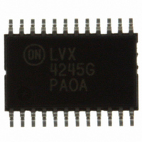
MC74LVX4245DTG
Manufacturer Part Number
MC74LVX4245DTG
Description
IC TXRX DUAL OCT 3ST LV 24TSSOP
Manufacturer
ON Semiconductor
Series
LVXr
Type
Transceiverr
Datasheet
1.MC74LVX4245DTR2G.pdf
(10 pages)
Specifications of MC74LVX4245DTG
Number Of Drivers/receivers
8/8
Voltage - Supply
2.7 V ~ 5.5 V
Mounting Type
Surface Mount
Package / Case
24-TSSOP
Logic Type
CMOS
Logic Family
74LVX
Number Of Channels Per Chip
8
Input Level
CMOS
Output Level
CMOS
Output Type
3-State
High Level Output Current
- 24 mA
Low Level Output Current
24 mA
Propagation Delay Time
10 ns
Supply Voltage (max)
3.6 V, 5.5 V
Supply Voltage (min)
2.7 V, 4.5 V
Maximum Operating Temperature
+ 85 C
Function
Bus Transceiver with Voltage Translation
Input Bias Current (max)
8 uA
Maximum Power Dissipation
200 mW
Minimum Operating Temperature
- 40 C
Mounting Style
SMD/SMT
Number Of Circuits
2
Polarity
Non-Inverting
Operating Supply Voltage (typ)
3.3/5V
Number Of Elements
1
Number Of Channels
8
Input Logic Level
CMOS
Output Logic Level
CMOS
Package Type
TSSOP
Logical Function
Bus Transceiver with Voltage Translation
Operating Supply Voltage (min)
2.7/4.5V
Technology
CMOS
Operating Temp Range
-40C to 85C
Operating Temperature Classification
Industrial
Mounting
Surface Mount
Additional Features
W/Volt Translation
Pin Count
24
Lead Free Status / RoHS Status
Lead free / RoHS Compliant
Protocol
-
Lead Free Status / Rohs Status
Lead free / RoHS Compliant
Other names
MC74LVX4245DTGOS


1. Worst case package.
2. Max number of outputs defined as (n). Data inputs are driven 0V to V
3. Max number of data inputs (n) switching. (n−1) inputs switching 0V to V
DC ELECTRICAL CHARACTERISTICS
CAPACITIVE CHARACTERISTICS
Symbol
Symbol
V
V
V
V
V
V
V
V
DI
I
I
I
I
C
C
0V to threshold (V
CCA
CCB
OLPA
OLPB
OLVB
C
OZA
OZB
OLVA
IHDA
IHDB
ILDA
ILDB
I
IN
PD
I/O
CC
IN
Input Capacitance
Input/Output Capacitance
Power Dissipation Capacitance
(Measured at 10MHz)
Max Input Leak-
age
Current
Max 3−State Out-
put Leakage
Max 3−State Out-
put Leakage
Maximum I
per Input
Quiescent V
Supply Current
Quiescent V
Supply Current
Quiet Output Max
Dynamic V
Quiet Output Min
Dynamic V
Min HIGH Level
Dynamic Input
Voltage
Max LOW Level
Dynamic Input
Voltage
Parameter
ILD
CCT
OL
OL
), f = 1MHz.
CCA
CCB
Parameter
An,OE
OE,
T/R
T/R
An
Bn
Bn
An=V
Bn=V
An=V
Bn=V
V
V
V
V
V
O
O
I
V
V
I
I
OE = V
OE = V
= V
=V
=V
Condition
T/R=V
Notes 1, 2
Notes 1, 2
Notes 1, 3
Notes 1, 3
= V
= V
T/R=GND
OE=GND
OE=GND
I
I
= V
= V
CCA
CCB
CCA
CCB
CCA
CCB
CCA
CCA
CCB
IH
IH
or GND
or GND
or GND
or GND
−2.1V
−0.6V
CCA
CCA
CCA
, GND
, V
, V
, GND
, GND
IL
IL
B A
A B
http://onsemi.com
MC74LVX4245
V
5.5
5.5
5.5
5.5
5.5
5.5
5.5
5.0
5.0
5.0
5.0
5.0
5.0
5.0
5.0
CCA
4
V
V
CCA
CCA
CC
CC
V
level; one output at GND.
3.6
3.6
3.6
3.6
3.6
3.6
3.6
3.3
3.3
3.3
3.3
3.3
3.3
3.3
3.3
= 5.0V; V
= 5.0V; V
CCB
V
V
level. Input under test switching: V
Condition
CCA
CCB
= 5.0V
= 3.3V
Typ
1.0
CCB
CCB
T
A
= 25 C
= 3.3V
= 3.3V
1.35
0.35
−1.2
−0.8
1.5
1.2
2.0
2.0
0.8
0.8
0.1
0.5
0.5
8
5
Guaranteed Limits
T
A
= −40 to +85 C
CC
Typical
1.5
0.5
4.5
80
50
15
55
40
1.0
5.0
5.0
level to threshold (V
Unit
Unit
mA
mA
mA
mA
mA
mA
mA
pF
pF
pF
V
V
V
V
IHD
),
Related parts for MC74LVX4245DTG
Image
Part Number
Description
Manufacturer
Datasheet
Request
R

Part Number:
Description:
ON Semiconductor [VOLTAGE REGULATOR]
Manufacturer:
ON Semiconductor
Datasheet:
Part Number:
Description:
357-036-542-201 CARDEDGE 36POS DL .156 BLK LOPRO
Manufacturer:
ON Semiconductor
Datasheet:
Part Number:
Description:
357-036-542-201 CARDEDGE 36POS DL .156 BLK LOPRO
Manufacturer:
ON Semiconductor
Datasheet:
Part Number:
Description:
357-036-542-201 CARDEDGE 36POS DL .156 BLK LOPRO
Manufacturer:
ON Semiconductor
Datasheet:
Part Number:
Description:
357-036-542-201 CARDEDGE 36POS DL .156 BLK LOPRO
Manufacturer:
ON Semiconductor
Datasheet:
Part Number:
Description:
357-036-542-201 CARDEDGE 36POS DL .156 BLK LOPRO
Manufacturer:
ON Semiconductor
Datasheet:
Part Number:
Description:
357-036-542-201 CARDEDGE 36POS DL .156 BLK LOPRO
Manufacturer:
ON Semiconductor
Datasheet:
Part Number:
Description:
357-036-542-201 CARDEDGE 36POS DL .156 BLK LOPRO
Manufacturer:
ON Semiconductor
Datasheet:
Part Number:
Description:
357-036-542-201 CARDEDGE 36POS DL .156 BLK LOPRO
Manufacturer:
ON Semiconductor
Datasheet:
Part Number:
Description:
357-036-542-201 CARDEDGE 36POS DL .156 BLK LOPRO
Manufacturer:
ON Semiconductor
Datasheet:
Part Number:
Description:
357-036-542-201 CARDEDGE 36POS DL .156 BLK LOPRO
Manufacturer:
ON Semiconductor
Datasheet:
Part Number:
Description:
Manufacturer:
ON Semiconductor
Datasheet:
Part Number:
Description:
Manufacturer:
ON Semiconductor
Datasheet:
Part Number:
Description:
Manufacturer:
ON Semiconductor
Datasheet: