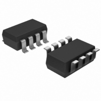
MAX9111EKA+T Maxim Integrated Products, MAX9111EKA+T Datasheet - Page 5

MAX9111EKA+T
Manufacturer Part Number
MAX9111EKA+T
Description
IC RCVR SNGL LVDS SOT23-8
Manufacturer
Maxim Integrated Products
Type
Receiverr
Specifications of MAX9111EKA+T
Number Of Drivers/receivers
0/1
Protocol
LVDS
Voltage - Supply
3 V ~ 3.6 V
Mounting Type
Surface Mount
Package / Case
SOT-23-8
Logic Family
MAX9111
Logic Type
LVDS Line Receiver
Supply Voltage (max)
4 V
Supply Voltage (min)
- 0.3 V
Maximum Operating Temperature
+ 85 C
Mounting Style
SMD/SMT
Data Rate
500 Mbps
Maximum Power Dissipation
714 mW
Minimum Operating Temperature
- 40 C
Output Voltage
+/- 0.3 V
Propagation Delay Time
1.77 ns
Supply Current
4.2 mA
Lead Free Status / RoHS Status
Lead free / RoHS Compliant
The MAX9110/MAX9112 single/dual LVDS transmitters
are intended for high-speed, point-to-point, low-power
applications. These devices accept CMOS/LVTTL
inputs with data rates exceeding 500Mbps. The
MAX9110/MAX9112 reduce power consumption and
(V
CC
SOT23
3, 5, 6
= +3.3V, R
—
—
—
4
1
2
7
8
MAX9110
1.45
1.44
1.43
1.42
1.41
1.40
1.39
1.38
1.37
1.36
1.35
L
75.0
= 100Ω, C
_______________________________________________________________________________________
3, 5, 6
SO
87.5
—
—
—
1
2
4
7
8
V
OUTPUT HIGH VOLTAGE
Detailed Description
vs. LOAD RESISTANCE
CC
V
LOAD RESISTANCE (Ω)
L
100.0
CC
= +3.3V
= 5pF, V
= +3.6V
PIN
112.5 125.0 137.5 150.0
Single/Dual LVDS Line Drivers with
SOT23
IH
V
1, 3
6, 7
5, 8
CC
—
—
—
—
4
2
= +3V, V
= +3V
MAX9112
Ultra-Low Pulse Skew in SOT23
Typical Operating Characteristics (continued)
IL
= GND, f
2, 3
6, 7
5, 8
SO
—
—
—
—
1
4
IN
= 20MHz, T
DO2+, DO1+
DO2-, DO1-
DIN1, DIN2
EMI by translating these signals to a differential voltage
in the 250mV to 450mV range across a 100Ω load while
drawing only 9.4mA of supply current for the dual-
channel MAX9112.
A current-steering approach induces less ground
bounce and no shoot-through current, enhancing noise
margin and system speed performance. The output
NAME
GND
DO+
N.C.
V
DIN
DO-
CC
A
= +25°C, unless otherwise noted.) (Figures 2, 3)
1.10
1.09
1.08
1.07
1.06
1.05
1.04
1.03
1.02
1.01
1.00
75.0
Positive Supply
Transmitter Input
No Connection. Not internally connected.
Ground
Noninverting Transmitter Output
Inverting Transmitter Output
V
87.5
CC
= +3V
OUTPUT LOW VOLTAGE
vs. LOAD RESISTANCE
LOAD RESISTANCE (Ω)
100.0
112.5 125.0 137.5 150.0
V
CC
FUNCTION
= +3.3V
V
Pin Description
CC
= +3.6V
5


