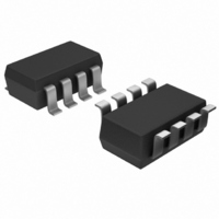
MAX9111EKA+T Maxim Integrated Products, MAX9111EKA+T Datasheet - Page 6

MAX9111EKA+T
Manufacturer Part Number
MAX9111EKA+T
Description
IC RCVR SNGL LVDS SOT23-8
Manufacturer
Maxim Integrated Products
Type
Receiverr
Specifications of MAX9111EKA+T
Number Of Drivers/receivers
0/1
Protocol
LVDS
Voltage - Supply
3 V ~ 3.6 V
Mounting Type
Surface Mount
Package / Case
SOT-23-8
Logic Family
MAX9111
Logic Type
LVDS Line Receiver
Supply Voltage (max)
4 V
Supply Voltage (min)
- 0.3 V
Maximum Operating Temperature
+ 85 C
Mounting Style
SMD/SMT
Data Rate
500 Mbps
Maximum Power Dissipation
714 mW
Minimum Operating Temperature
- 40 C
Output Voltage
+/- 0.3 V
Propagation Delay Time
1.77 ns
Supply Current
4.2 mA
Lead Free Status / RoHS Status
Lead free / RoHS Compliant
stage presents a symmetrical, high-impedance output,
reducing differential reflection and timing distortion. The
driver outputs are short circuit current limited and enter a
high-impedance state when the device is not powered.
The LVDS interface standard is a signaling method
intended for point-to-point communication over a con-
trolled impedance medium as defined by the EIA/TIA-
644 LVDS standard. The LVDS standard uses a lower
voltage swing than other common communication stan-
dards, achieving higher data rates with reduced power
consumption while reducing EMI emissions and system
susceptibility to noise.
LVDS transmitters such as the MAX9110/MAX9112
convert CMOS/LVTTL signals to low-voltage differential
signals at rates in excess of 500Mbps. The MAX9110/
MAX9112 current-steering architecture requires a resis-
tive load to terminate the signal and complete the trans-
Single/Dual LVDS Line Drivers with
Ultra-Low Pulse Skew in SOT23
Figure 1. LVDS Transmitter V
Figure 3. Transmitter Propagation Delay and Transition Time Waveforms
6
_______________________________________________________________________________________
GND
V
CC
DIN_
OD
DO_ -
DO_+
V
DIN_
DIFF
R
and V
R
L
L
/2
/2
DO_+
DO_-
OS
V
LVDS Operation
OS
Test Circuit
20%
1.5V
t
PLHD
V
OD
t
TLH
0V DIFFERENTIAL
80%
0
V
DIFF
= V
DO_
mission loop. Because the device switches the direc-
tion of current flow and not voltage levels, the actual
output voltage swing is determined by the value of the
termination resistor at the input of an LVDS receiver.
Logic states are determined by the direction of current
flow through the termination resistor. With a typical
3.5mA output current, the MAX9110/MAX9112 produce
an output voltage of 350mV when driving a 100Ω load.
The steady-state-voltage peak-to-peak swing is twice
the differential voltage, or 700mV (typ).
Bypass V
0.1µF and 0.001µF capacitors in parallel, as close to the
device as possible, with the smaller valued capacitor the
closest. For additional supply bypassing, place a 10µF
tantalum or ceramic capacitor at the point where power
enters the circuit board.
+ - V
Figure 2. Transmitter Propagation Delay and Transition Time
Test Circuit
DO_
GENERATOR
-
80%
1.5V
t
PHLD
CC
t
THL
with high-frequency surface-mount ceramic
Applications Information
50Ω
0
0
DIN_
20%
V
V
3V
0
OH
OL
C
C
Supply Bypassing
L
L
R
L
DO_ +
DO_ -


