J308-E3 Vishay, J308-E3 Datasheet - Page 3
J308-E3
Manufacturer Part Number
J308-E3
Description
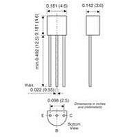
TRANSISTOR,JFET,N-Channel,25V,12mA, TO-92
Manufacturer
Vishay
Datasheet
1.J308-E3.pdf
(8 pages)
Specifications of J308-E3
Power Dissipation Pd
350mW
Transistor Polarity
N Channel
Current Rating
10mA
Continuous Drain Current Id
60mA
Gate-source Breakdown Voltage
-25V
Leaded Process Compatible
Yes
Rohs Compliant
Yes
Mounting Type
Through Hole
Gate-source Cutoff Voltage
-6.5V


Notes
a.
b.
c.
d.
Stresses beyond those listed under “Absolute Maximum Ratings” may cause permanent damage to the device. These are stress ratings only, and functional operation
of the device at these or any other conditions beyond those indicated in the operational sections of the specifications is not implied. Exposure to absolute maximum
rating conditions for extended periods may affect device reliability.
SPECIFICATIONS FOR U309 AND U310 (T
Static
Gate-Source Breakdown Voltage
Gate-Source Cutoff Voltage
Saturation Drain Current
Gate Reverse Current
Gate Reverse Current
Gate Operating Current
Drain-Source On-Resistance
Gate-Source Forward Voltage
Dynamic
Common-Source
Forward Transconductance
Common-Source
Output Conductance
Common-Source
Input Capacitance
Common-Source
Reverse Transfer Capacitance
Equivalent Input Noise Voltage
High Frequency
Common-Gate
Common-Gate
Forward Transconductance
Common-Gate
Common-Gate
Output Conductance
Common Gate Power Gain
Common-Gate Power Gain
Noise Figure
Noise Figure
Document Number: 70237
S-50149—Rev. H, 24-Jan-05
Typical values are for DESIGN AID ONLY, not guaranteed nor subject to production testing.
Pulse test: PW v300 ms duty cycle v3%.
Gain (G
Not a production test.
pg
d
d
Parameter
) measured at optimum input noise match.
b
c, d
c, d
Symbol
V
V
r
(BR)GSS
V
DS(on)
GS(off)
I
I
I
C
C
G
G
DSS
GSS
GSS
GS(F)
g
g
g
g
g
NF
NF
g
I
e
rss
og
G
os
iss
fs
f
fg
pg
n
V
V
I
D
DS
DS
= 10 mA
V
V
= 10 V
= 10 V
V
V
V
V
I
I
V
V
DS
DS
Test Conditions
V
G
G
V
DS
DS
DS
GS
DS
DG
DS
GS
= 10 mA , V
A
= −1 mA , V
= 10 V, V
= 10 V, V
= 10 V, I
= 10 V, I
= 10 V, I
= −15 V, V
= 10 V, V
= 9 V, I
= 10 V, I
= 0 V, I
= 25_C UNLESS NOTED)
f = 1 MHz
f = 100 Hz
f = 1 kHz
D
D
D
D
D
GS
GS
D
DS
GS
= 10 mA
DS
= 1 mA
DS
= 10 mA
= 10 mA
= 10 mA
= 1 nA
= −10 V
= −10 V
f = 105 MHz
f = 450 MHz
f = 105 MHz
f = 450 MHz
f = 105 MHz
f = 450 MHz
f = 105 MHz
f = 450 MHz
= 0 V
= 0 V
T
= 0 V
= 0 V
A
= 125_C
−0.002
−0.001
Typ
0.16
0.55
11.5
−35
−15
110
0.7
1.9
1.5
2.7
35
14
14
13
16
4
6
a
J/SST/U308 Series
Min
−25
−1
12
10
14
10
U309
Max
−
−
250
Vishay Siliconix
0.15
0.15
2.5
3.5
−4
30
1
5
2
Limits
Min
−2.5
−25
24
10
14
10
U310
Max
−
−
www.vishay.com
250
2.5
3.5
60
0.15
0.15
−6
1
5
2
Unit
√Hz
mA
mS
nV⁄
mS
mS
nA
mA
pA
mS
dB
dB
pF
pF
W
V
V
V
NZB
3
Related parts for J308-E3
Image
Part Number
Description
Manufacturer
Datasheet
Request
R


Part Number:
Description:
357-036-542-201 CARDEDGE 36POS DL .156 BLK LOPRO
Manufacturer:
Vishay
Datasheet:
Part Number:
Description:
357-036-542-201 CARDEDGE 36POS DL .156 BLK LOPRO
Manufacturer:
Vishay
Datasheet:
Part Number:
Description:
357-036-542-201 CARDEDGE 36POS DL .156 BLK LOPRO
Manufacturer:
Vishay
Datasheet:
Part Number:
Description:
357-036-542-201 CARDEDGE 36POS DL .156 BLK LOPRO
Manufacturer:
Vishay
Datasheet:
Part Number:
Description:
357-036-542-201 CARDEDGE 36POS DL .156 BLK LOPRO
Manufacturer:
Vishay
Datasheet:
Part Number:
Description:
357-036-542-201 CARDEDGE 36POS DL .156 BLK LOPRO
Manufacturer:
Vishay
Datasheet:
Part Number:
Description:
357-036-542-201 CARDEDGE 36POS DL .156 BLK LOPRO
Manufacturer:
Vishay
Datasheet:
Part Number:
Description:
357-036-542-201 CARDEDGE 36POS DL .156 BLK LOPRO
Manufacturer:
Vishay
Datasheet:
Part Number:
Description:
357-036-542-201 CARDEDGE 36POS DL .156 BLK LOPRO
Manufacturer:
Vishay
Datasheet:
Part Number:
Description:
357-036-542-201 CARDEDGE 36POS DL .156 BLK LOPRO
Manufacturer:
Vishay
Datasheet:
Part Number:
Description:
357-036-542-201 CARDEDGE 36POS DL .156 BLK LOPRO
Manufacturer:
Vishay
Datasheet:
Part Number:
Description:
357-036-542-201 CARDEDGE 36POS DL .156 BLK LOPRO
Manufacturer:
Vishay
Datasheet:
Part Number:
Description:
357-036-542-201 CARDEDGE 36POS DL .156 BLK LOPRO
Manufacturer:
Vishay
Datasheet:
Part Number:
Description:
357-036-542-201 CARDEDGE 36POS DL .156 BLK LOPRO
Manufacturer:
Vishay
Datasheet: