J308-E3 Vishay, J308-E3 Datasheet - Page 6
J308-E3
Manufacturer Part Number
J308-E3
Description
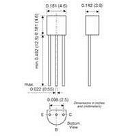
TRANSISTOR,JFET,N-Channel,25V,12mA, TO-92
Manufacturer
Vishay
Datasheet
1.J308-E3.pdf
(8 pages)
Specifications of J308-E3
Power Dissipation Pd
350mW
Transistor Polarity
N Channel
Current Rating
10mA
Continuous Drain Current Id
60mA
Gate-source Breakdown Voltage
-25V
Leaded Process Compatible
Yes
Rohs Compliant
Yes
Mounting Type
Through Hole
Gate-source Cutoff Voltage
-6.5V


J/SST/U308 Series
Vishay Siliconix
www.vishay.com
6
TYPICAL CHARACTERISTICS (T
100
100
0.1
80
60
40
20
15
12
10
0
9
6
3
0
1
100
1
0
f = 1 MHz
T
V
I
Common−Gate
D
A
DG
V
= 10 mA
= 25_C
Common-Source Input Capacitance
g
DS
V
= 10 V
On-Resistance vs. Drain Current
ig
Input Admittance vs. Frequency
GS(off)
= 0 V
−4
V
vs. Gate-Source Voltage
GS
= −1.5 V
200
I
− Gate-Source Voltage (V)
D
f − Frequency (MHz)
− Drain Current (mA)
−8
b
ig
V
10
DS
= 5 V
−12
V
500
GS(off)
−16
= −3 V
A
= 25_C UNLESS OTHERWISE NOTED)
1000
100
−20
100
0.1
10
100
1
80
60
40
20
10
0
8
6
4
2
0
Common-Source Reverse Feedback Capacitance
0.1
100
0
T
V
I
Common−Gate
f = 1 MHz
D
A
DG
V
Circuit Voltage Gain vs. Drain Current
= 10 mA
= 25_C
DS
Forward Admittance vs. Frequency
= 10 V
= 0 V
−4
V
−g
DS
V
vs. Gate-Source Voltage
fg
GS
= 5 V
200
I
Assume V
A
R
D
− Gate-Source Voltage (V)
f − Frequency (MHz)
V
L
− Drain Current (mA)
+
+
−8
10 V
1 ) R
I
D
DD
g
1
V
fs
S-50149—Rev. H, 24-Jan-05
= 15 V, V
GS(off)
R
L
−12
L
b
Document Number: 70237
g
fg
os
= −3 V
V
500
GS(off)
DS
= 5 V
−16
= −1.5 V
1000
−20
10
Related parts for J308-E3
Image
Part Number
Description
Manufacturer
Datasheet
Request
R


Part Number:
Description:
357-036-542-201 CARDEDGE 36POS DL .156 BLK LOPRO
Manufacturer:
Vishay
Datasheet:
Part Number:
Description:
357-036-542-201 CARDEDGE 36POS DL .156 BLK LOPRO
Manufacturer:
Vishay
Datasheet:
Part Number:
Description:
357-036-542-201 CARDEDGE 36POS DL .156 BLK LOPRO
Manufacturer:
Vishay
Datasheet:
Part Number:
Description:
357-036-542-201 CARDEDGE 36POS DL .156 BLK LOPRO
Manufacturer:
Vishay
Datasheet:
Part Number:
Description:
357-036-542-201 CARDEDGE 36POS DL .156 BLK LOPRO
Manufacturer:
Vishay
Datasheet:
Part Number:
Description:
357-036-542-201 CARDEDGE 36POS DL .156 BLK LOPRO
Manufacturer:
Vishay
Datasheet:
Part Number:
Description:
357-036-542-201 CARDEDGE 36POS DL .156 BLK LOPRO
Manufacturer:
Vishay
Datasheet:
Part Number:
Description:
357-036-542-201 CARDEDGE 36POS DL .156 BLK LOPRO
Manufacturer:
Vishay
Datasheet:
Part Number:
Description:
357-036-542-201 CARDEDGE 36POS DL .156 BLK LOPRO
Manufacturer:
Vishay
Datasheet:
Part Number:
Description:
357-036-542-201 CARDEDGE 36POS DL .156 BLK LOPRO
Manufacturer:
Vishay
Datasheet:
Part Number:
Description:
357-036-542-201 CARDEDGE 36POS DL .156 BLK LOPRO
Manufacturer:
Vishay
Datasheet:
Part Number:
Description:
357-036-542-201 CARDEDGE 36POS DL .156 BLK LOPRO
Manufacturer:
Vishay
Datasheet:
Part Number:
Description:
357-036-542-201 CARDEDGE 36POS DL .156 BLK LOPRO
Manufacturer:
Vishay
Datasheet:
Part Number:
Description:
357-036-542-201 CARDEDGE 36POS DL .156 BLK LOPRO
Manufacturer:
Vishay
Datasheet: