DS21348G Maxim Integrated Products, DS21348G Datasheet - Page 32
DS21348G
Manufacturer Part Number
DS21348G
Description
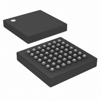
IC LIU T1/E1/J1 3.3V 49-BGA
Manufacturer
Maxim Integrated Products
Type
Line Interface Units (LIUs)r
Datasheet
1.DS21348G.pdf
(76 pages)
Specifications of DS21348G
Number Of Drivers/receivers
1/1
Protocol
T1/E1/J1
Voltage - Supply
3.135 V ~ 3.465 V
Mounting Type
Surface Mount
Package / Case
49-CSBGA
Lead Free Status / RoHS Status
Contains lead / RoHS non-compliant
Available stocks
Company
Part Number
Manufacturer
Quantity
Price

Part Number:
DS21348G
Manufacturer:
NXP/恩智浦
Quantity:
20 000
Part Number:
DS21348G+
Manufacturer:
MAXIM/美信
Quantity:
20 000
Company:
Part Number:
DS21348GN-C01
Manufacturer:
Maxim Integrated
Quantity:
10 000


4.1 Device Power-Up and Reset
The DS21348 will reset itself upon power-up setting all writeable registers to 00h and clear the status and
information registers. CCR3.7 (TUA1) = 0 results in the LIU transmitting unframed all ones. After the
power supplies have settled following power-up, initialize all control registers to the desired settings, then
toggle the LIRST bit (CCR3.2). At anytime, the DS21348 can be reset to the default settings by bringing
HRST (pin 29) low (level triggered) or by powering down and powering up again.
CCR4 (03H): COMMON CONTROL REGISTER 4
Table 4-2. Receive Equalizer Sensitivity Settings
(CCR4.4)
SYMBOL
JABDS
(MSB)
EGL
EGL
TPD
DJA
JAS
L2
L2
L1
L0
0
1
1
0
POSITION
(CCR1.7)
0 (E1)
0 (E1)
1 (T1)
1 (T1)
CCR4.7
CCR4.6
CCR4.5
CCR4.4
CCR4.3
CCR4.2
CCR4.1
CCR4.0
L1
ETS
-12dB (short haul)
-43dB (long haul)
-30dB (limited long haul)
-36dB (long haul)
DESCRIPTION
Line Build Out Select Bit 2. Sets the transmitter build out; see
for E1 and
Line Build Out Select Bit 1. Sets the transmitter build out; see
for E1 and
Line Build Out Select Bit 0. Sets the transmitter build out; see
for E1 and
Receive Equalizer Gain Limit. This bit controls the sensitivity of the
receive equalizer. See
Jitter Attenuator Select.
0 = place the jitter attenuator on the receive side
1 = place the jitter attenuator on the transmit side
Jitter Attenuator Buffer Depth Select.
0 = 128 bits
1 = 32 bits (use for delay-sensitive applications)
Disable Jitter Attenuator.
0 = jitter attenuator enabled
1 = jitter attenuator disabled
Transmit Power-Down.
0 = normal transmitter operation
1 = powers down the transmitter and tri-states the TTIP and TRING pins
L0
SENSITIVITY
RECEIVE
Table 7-2
Table 7-2
Table 7-2
EGL
32 of 76
for T1.
for T1.
for T1.
Table
JAS
4-2.
JABDS
DJA
Table 7-1
Table 7-1
Table 7-1
(LSB)
TPD
Related parts for DS21348G
Image
Part Number
Description
Manufacturer
Datasheet
Request
R

Part Number:
Description:
MAX7528KCWPMaxim Integrated Products [CMOS Dual 8-Bit Buffered Multiplying DACs]
Manufacturer:
Maxim Integrated Products
Datasheet:
Part Number:
Description:
Single +5V, fully integrated, 1.25Gbps laser diode driver.
Manufacturer:
Maxim Integrated Products
Datasheet:
Part Number:
Description:
Single +5V, fully integrated, 155Mbps laser diode driver.
Manufacturer:
Maxim Integrated Products
Datasheet:
Part Number:
Description:
VRD11/VRD10, K8 Rev F 2/3/4-Phase PWM Controllers with Integrated Dual MOSFET Drivers
Manufacturer:
Maxim Integrated Products
Datasheet:
Part Number:
Description:
Highly Integrated Level 2 SMBus Battery Chargers
Manufacturer:
Maxim Integrated Products
Datasheet:
Part Number:
Description:
Current Monitor and Accumulator with Integrated Sense Resistor; ; Temperature Range: -40°C to +85°C
Manufacturer:
Maxim Integrated Products
Part Number:
Description:
TSSOP 14/A�/RS-485 Transceivers with Integrated 100O/120O Termination Resis
Manufacturer:
Maxim Integrated Products
Part Number:
Description:
TSSOP 14/A�/RS-485 Transceivers with Integrated 100O/120O Termination Resis
Manufacturer:
Maxim Integrated Products
Part Number:
Description:
QFN 16/A�/AC-DC and DC-DC Peak-Current-Mode Converters with Integrated Step
Manufacturer:
Maxim Integrated Products
Part Number:
Description:
TDFN/A/65V, 1A, 600KHZ, SYNCHRONOUS STEP-DOWN REGULATOR WITH INTEGRATED SWI
Manufacturer:
Maxim Integrated Products
Part Number:
Description:
Integrated Temperature Controller f
Manufacturer:
Maxim Integrated Products
Part Number:
Description:
SOT23-6/I�/45MHz to 650MHz, Integrated IF VCOs with Differential Output
Manufacturer:
Maxim Integrated Products
Part Number:
Description:
SOT23-6/I�/45MHz to 650MHz, Integrated IF VCOs with Differential Output
Manufacturer:
Maxim Integrated Products
Part Number:
Description:
EVALUATION KIT/2.4GHZ TO 2.5GHZ 802.11G/B RF TRANSCEIVER WITH INTEGRATED PA
Manufacturer:
Maxim Integrated Products
Part Number:
Description:
QFN/E/DUAL PCIE/SATA HIGH SPEED SWITCH WITH INTEGRATED BIAS RESISTOR
Manufacturer:
Maxim Integrated Products
Datasheet: