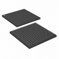
DS26514GN+ Maxim Integrated Products, DS26514GN+ Datasheet - Page 24

DS26514GN+
Manufacturer Part Number
DS26514GN+
Description
IC TXRX T1/E1/J1 4PORT 256-CSBGA
Manufacturer
Maxim Integrated Products
Type
Transceiverr
Datasheet
1.DS26514GN.pdf
(305 pages)
Specifications of DS26514GN+
Number Of Drivers/receivers
4/4
Protocol
Ethernet
Voltage - Supply
3.14 V ~ 3.47 V
Mounting Type
Surface Mount
Package / Case
256-CSBGA
Lead Free Status / RoHS Status
Lead free / RoHS Compliant
- Current page: 24 of 305
- Download datasheet (2Mb)
Rev: 101608
D[6]/SPI_CPHA
D[7]/SPI_CPOL
RCHBLK1/
RCHBLK2/
RCHBLK3/
RCHBLK4/
RCHCLK1
RCHCLK2
RCHCLK3
RCHCLK4
RLF/LTC1
BPCLK1
NAME
CLKO/
A12
A11
A10
A9
A8
A7
A6
A5
A4
A3
A2
A1
A0
B10
A10
C10
PIN
E4
B5
D3
C8
A8
B8
B9
A9
C9
D9
E9
N9
L6
T5
E8
F8
F9
T9
Output
Output
Output
Output
Output
TYPE
Input/
Input/
Input
MICROPROCESSOR INTERFACE
Receive Channel Block/Receive Channel Block Clock. This pin can be
configured to output either RCHBLK or RCHCLK.
RCHBLK[1:4]. RCHBLKn is a user-programmable output that can be forced high
or low during any of the 24 T1 or 32 E1 channels. It is synchronous with RCLKn
when the receive-side elastic store is disabled. It is synchronous with RSYSCLKn
when the receive-side elastic store is enabled. This pin is useful for blocking
clocks to a serial UART or LAPD controller in applications where not all channels
are used such as fractional service, 384kbps service, 768kbps, or ISDN-PRI. Also
useful for locating individual channels in drop-and-insert applications, for external
per-channel loopback, and for per-channel conditioning.
RCHCLK[1:4]. RCHCLKn is a 192kHz (T1) or 256kHz (E1) clock that pulses high
during the LSB of each channel. It is synchronous with RCLKn when the receive-
side elastic store is disabled. It is synchronous with RSYSCLKn when the
receive-side elastic store is enabled. It is useful for parallel-to-serial conversion of
channel data.
Backplane Clock 1. Programmable clock output that can be set to 2.048MHz,
4.096MHz, 8.192MHz, or 16.384MHz. The reference for this clock can be
RCLK[8:1], a 1.544MHz or 2.048MHz clock frequency derived from MCLK, or an
external reference clock (REFCLKIO). This allows system clocks to be referenced
from external sources, the T1J1E1 recovered clocks, or the MCLK oscillator.
Clock Out. Clock output pin that can be programmed to output numerous
frequencies referenced to MCLK. Frequencies available: 1.544MHz, 2.048MHz,
4.096MHz, 8.192MHz, 12.288MHz, 16.384MHz, 256kHz, and 64kHz.
GTCCR3.CLKOSEL[2:0] selects the frequency.
Receive Loss of Frame/Loss of Transmit Clock. This pin can also be
programmed to either toggle high when the synchronizer is searching for the
frame and multiframe, or to toggle high if the TCLKn pin has not been toggled for
approximately three clock periods.
RLF/LTC1 is available on the DS26514 when GTCR1.528MD = 1.
Address [12:0]. This bus selects a specific register in the DS26514 during
read/write access. A12 is the MSB and A0 is the LSB.
Data [7]/SPI Interface Clock Polarity
D[7]: Bit 7 of the 16-bit or 8-bit data bus used to input data during register writes
and data outputs during register reads. Not driven when CSB = 1.
SPI_CPOL: This signal selects the clock polarity when SPI_SEL = 1. See Section
9.1.2
Data [6]/SPI Interface Clock Phase
D[6]: Bit 6 of the 16-bit or 8-bit data bus used to input data during register writes
and data outputs during register reads. Not driven when CSB = 1.
SPI_CPHA: This signal selects the clock phase when SPI_SEL = 1. See Section
9.1.2
for detailed timing and functionality information. Default setting is low.
for detailed timing and functionality information. Default setting is low.
FUNCTION
DS26514 4-Port T1/E1/J1 Transceiver
24 of 305
Related parts for DS26514GN+
Image
Part Number
Description
Manufacturer
Datasheet
Request
R

Part Number:
Description:
4-port T1/e1/j1 Transceiver
Manufacturer:
Maxim Integrated Products, Inc.
Datasheet:

Part Number:
Description:
power light source LUXEON® Collimator
Manufacturer:
LUMILEDS [Lumileds Lighting Company]
Datasheet:

Part Number:
Description:
MAX7528KCWPMaxim Integrated Products [CMOS Dual 8-Bit Buffered Multiplying DACs]
Manufacturer:
Maxim Integrated Products
Datasheet:

Part Number:
Description:
Single +5V, fully integrated, 1.25Gbps laser diode driver.
Manufacturer:
Maxim Integrated Products
Datasheet:

Part Number:
Description:
Single +5V, fully integrated, 155Mbps laser diode driver.
Manufacturer:
Maxim Integrated Products
Datasheet:

Part Number:
Description:
VRD11/VRD10, K8 Rev F 2/3/4-Phase PWM Controllers with Integrated Dual MOSFET Drivers
Manufacturer:
Maxim Integrated Products
Datasheet:

Part Number:
Description:
Highly Integrated Level 2 SMBus Battery Chargers
Manufacturer:
Maxim Integrated Products
Datasheet:

Part Number:
Description:
Current Monitor and Accumulator with Integrated Sense Resistor; ; Temperature Range: -40°C to +85°C
Manufacturer:
Maxim Integrated Products

Part Number:
Description:
TSSOP 14/A°/RS-485 Transceivers with Integrated 100O/120O Termination Resis
Manufacturer:
Maxim Integrated Products

Part Number:
Description:
TSSOP 14/A°/RS-485 Transceivers with Integrated 100O/120O Termination Resis
Manufacturer:
Maxim Integrated Products

Part Number:
Description:
QFN 16/A°/AC-DC and DC-DC Peak-Current-Mode Converters with Integrated Step
Manufacturer:
Maxim Integrated Products

Part Number:
Description:
TDFN/A/65V, 1A, 600KHZ, SYNCHRONOUS STEP-DOWN REGULATOR WITH INTEGRATED SWI
Manufacturer:
Maxim Integrated Products

Part Number:
Description:
Integrated Temperature Controller f
Manufacturer:
Maxim Integrated Products

Part Number:
Description:
SOT23-6/I°/45MHz to 650MHz, Integrated IF VCOs with Differential Output
Manufacturer:
Maxim Integrated Products


