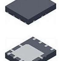
FDMS3602S Fairchild Semiconductor, FDMS3602S Datasheet - Page 13

FDMS3602S
Manufacturer Part Number
FDMS3602S
Description
MOSFET Power 25V Dual N-Channel PowerTrench MOSFET
Manufacturer
Fairchild Semiconductor
Datasheet
1.FDMS3602S.pdf
(15 pages)
Specifications of FDMS3602S
Configuration
Dual (MOSFET & SyncFET)
Transistor Polarity
Dual N-Channel
Resistance Drain-source Rds (on)
5.6 mOhms
Forward Transconductance Gfs (max / Min)
67 S
Drain-source Breakdown Voltage
25 V
Continuous Drain Current
15 A
Power Dissipation
2.2 W
Maximum Operating Temperature
+ 150 C
Mounting Style
SMD/SMT
Package / Case
Power 56
Module Configuration
Dual
Continuous Drain Current Id
40A
Drain Source Voltage Vds
25V
On Resistance Rds(on)
0.0044ohm
Rds(on) Test Voltage Vgs
10V
Lead Free Status / Rohs Status
Details
Following is a guideline, not a requirement which the PCB designer should consider:
1. Input ceramic bypass capacitors C1 and C2 must be placed close to the D1 and S2 pins of Power Stage to help reduce parasitic
inductance and high frequency conduction loss induced by switching operation. C1 and C2 show the bypass capacitors placed close
to the part between D1 and S2. Input capacitors should be connected in parallel close to the part. Multiple input caps can be connected
depending upon the application.
2. The PHASE copper trace serves two purposes; In addition to being the current path from the Power Stage package to the output
inductor (L), it also serves as heat sink for the lower FET in the Power Stage package. The trace should be short and wide enough to
present a low resistance path for the high current flow between the Power Stage and the inductor. This is done to minimize conduction
losses and limit temperature rise. Please note that the PHASE node is a high voltage and high frequency switching node with high
noise potential. Care should be taken to minimize coupling to adjacent traces. The reference layout in figure 31 shows a good balance
between the thermal and electrical performance of Power Stage.
3. Output inductor location should be as close as possible to the Power Stage device for lower power loss due to copper trace
resistance. A shorter and wider PHASE trace to the inductor reduces the conduction loss. Preferably the Power Stage should be
directly in line (as shown in figure 31) with the inductor for space savings and compactness.
®
4. The PowerTrench
Technology MOSFETs used in the Power Stage are effective at minimizing phase node ringing. It allows the
part to operate well within the breakdown voltage limits. This eliminates the need to have an external snubber circuit in most cases. If
the designer chooses to use an RC snubber, it should be placed close to the part between the PHASE pad and S2 pins to dampen
the high-frequency ringing.
5. The driver IC should be placed close to the Power Stage part with the shortest possible paths for the High Side gate and Low Side
gates through a wide trace connection. This eliminates the effect of parasitic inductance and resistance between the driver and the
MOSFET and turns the devices on and off as efficiently as possible. At higher-frequency operation this impedance can limit the gate
current trying to charge the MOSFET input capacitance. This will result in slower rise and fall times and additional switching losses.
Power Stage has both the gate pins on the same side of the package which allows for back mounting of the driver IC to the board. This
provides a very compact path for the drive signals and improves efficiency of the part.
6. S2 pins should be connected to the GND plane with multiple vias for a low impedance grounding. Poor grounding can create a noise
transient offset voltage level between S2 and driver ground. This could lead to faulty operation of the gate driver and MOSFET.
7. Use multiple vias on each copper area to interconnect top, inner and bottom layers to help smooth current flow and heat conduction.
Vias should be relatively large, around 8 mils to 10 mils, and of reasonable inductance. Critical high frequency components such as
ceramic bypass caps should be located close to the part and on the same side of the PCB. If not feasible, they should be connected
from the backside via a network of low inductance vias.
©2011 Fairchild Semiconductor Corporation
13
www.fairchildsemi.com
FDMS3602S Rev.C5


