PSMN5R0-100ES,127 NXP Semiconductors, PSMN5R0-100ES,127 Datasheet - Page 5
PSMN5R0-100ES,127
Manufacturer Part Number
PSMN5R0-100ES,127
Description
MOSFET Power N-Ch 100V 5 mOhms
Manufacturer
NXP Semiconductors
Series
-r
Datasheet
1.PSMN5R0-100ES127.pdf
(14 pages)
Specifications of PSMN5R0-100ES,127
Transistor Polarity
N-Channel
Resistance Drain-source Rds (on)
5 mOhms
Drain-source Breakdown Voltage
100 V
Gate-source Breakdown Voltage
20 V
Continuous Drain Current
110 A
Power Dissipation
338 W
Maximum Operating Temperature
+ 175 C
Mounting Style
SMD/SMT
Package / Case
I2PAK
Gate Charge Qg
170 nC
Minimum Operating Temperature
- 55 C
Fet Type
MOSFET N-Channel, Metal Oxide
Fet Feature
Standard
Rds On (max) @ Id, Vgs
5 mOhm @ 25A, 10V
Drain To Source Voltage (vdss)
100V
Current - Continuous Drain (id) @ 25° C
120A
Vgs(th) (max) @ Id
4V @ 1mA
Gate Charge (qg) @ Vgs
170nC @ 10V
Input Capacitance (ciss) @ Vds
9900pF @ 50V
Power - Max
338W
Mounting Type
Through Hole
Lead Free Status / Rohs Status
Details
Other names
934065165127


NXP Semiconductors
6. Characteristics
Table 6.
PSMN5R0-100ES
Product data sheet
Symbol
Static characteristics
V
V
V
I
I
R
R
Dynamic characteristics
Q
Q
Q
Q
Q
V
C
C
C
t
t
t
t
DSS
GSS
d(on)
r
d(off)
f
(BR)DSS
GS(th)
GS(th)
GS(pl)
DSon
G
iss
oss
rss
G(tot)
GS
GS(th)
GS(th-pl)
GD
Characteristics
Parameter
drain-source
breakdown voltage
gate-source threshold
voltage
gate-source threshold
voltage
drain leakage current
gate leakage current
drain-source on-state
resistance
gate resistance
total gate charge
gate-source charge
pre-threshold
gate-source charge
post-threshold
gate-source charge
gate-drain charge
gate-source plateau
voltage
input capacitance
output capacitance
reverse transfer
capacitance
turn-on delay time
rise time
turn-off delay time
fall time
Conditions
I
I
I
see
I
see
I
see
V
V
V
V
V
see
V
see
V
see
f = 1 MHz
I
see
I
see
I
see
I
see
V
see
V
T
V
R
All information provided in this document is subject to legal disclaimers.
D
D
D
D
D
D
D
D
D
j
DS
DS
GS
GS
GS
GS
GS
DS
DS
DS
G(ext)
= 25 °C; see
= 250 µA; V
= 250 µA; V
= 1 mA; V
= 1 mA; V
= 1 mA; V
= 75 A; V
= 0 A; V
= 75 A; V
= 75 A; V
Figure 10
Figure 10
Figure
Figure 12
Figure 12
Figure 13
Figure
Figure
Figure 15
Figure
Figure 15
= 100 V; V
= 100 V; V
= 50 V; see
= 50 V; V
= 50 V; R
= -20 V; V
= 20 V; V
= 10 V; I
= 10 V; I
= 10 V; I
= 4.7 Ω; I
Rev. 2 — 15 April 2011
DS
11; see
14; see
14; see
14; see
DS
DS
DS
DS
DS
DS
D
D
D
= 0 V; V
GS
DS
L
GS
GS
DS
= 25 A; T
= 25 A; T
= 25 A; T
= 50 V; V
= 50 V; V
= 50 V; V
GS
GS
= V
= V
= V
Figure 16
= 0.67 Ω; V
D
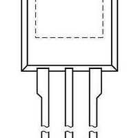
N-channel 100 V 5 mΩ standard level MOSFET in I2PAK
Figure
= 0 V; T
= 0 V; f = 1 MHz;
= 0 V; T
= 0 V; T
= 0 V; T
= 0 V; T
= 0 V; T
= 75 A; T
GS
GS
GS
Figure 10
Figure 15
Figure 15
Figure 15
; T
; T
; T
GS
14;
j
j
j
j
j
j
GS
GS
GS
= 10 V;
j
= 175 °C;
= -55 °C;
= 25 °C;
= 175 °C;
= 100 °C;
= 25 °C;
j
j
j
= 25 °C
j
j
= 25 °C
= -55 °C
= 25 °C
GS
= 25 °C
= 175 °C
= 10 V;
= 10 V;
= 10 V;
j
= 25 °C
= 10 V;
PSMN5R0-100ES
[1]
Min
100
90
1
-
2
-
-
-
-
-
-
-
-
-
-
-
-
-
-
-
-
-
-
-
-
-
-
Typ
-
-
-
-
3
0.08
-
10
10
12
7.7
4.3
0.9
170
140
48
31
17.3
49
5.1
9900
660
381
45
91
122
63
© NXP B.V. 2011. All rights reserved.
-
Max
-
-
-
4.6
4
10
500
100
100
14
9
5
-
-
-
-
-
-
-
-
-
-
-
-
-
-
Unit
V
V
V
V
V
µA
µA
nA
nA
mΩ
mΩ
mΩ
Ω
nC
C
nC
C
C
nC
V
pF
pF
pF
ns
ns
ns
ns
5 of 14
Related parts for PSMN5R0-100ES,127
Image
Part Number
Description
Manufacturer
Datasheet
Request
R

Part Number:
Description:
Standard level N-channel MOSFET in a I2PAK package qualified to 175 �C
Manufacturer:
NXP Semiconductors
Datasheet:

Part Number:
Description:
Standard level N-channel MOSFET in a TO-220 package qualified to 175 �C
Manufacturer:
NXP Semiconductors
Datasheet:

Part Number:
Description:
Logic level N-channel enhancement mode Field-Effect Transistor (FET) in a plastic package using TrenchMOS technology
Manufacturer:
NXP Semiconductors
Datasheet:
Part Number:
Description:
Standard level N-channel MOSFET in TO-220 package qualified to 175 �C
Manufacturer:
NXP Semiconductors
Datasheet:

Part Number:
Description:
MOSFET N-CH 30V 84A LFPAK
Manufacturer:
NXP Semiconductors
Datasheet:

Part Number:
Description:
Psmn5r0-100bs N-channel 100 V 5 M?? Standard Level Mosfet In D2pak
Manufacturer:
NXP Semiconductors
Datasheet:

Part Number:
Description:
MOSFET N-CH 80V 100A TO-220AB3
Manufacturer:
NXP Semiconductors
Datasheet:

Part Number:
Description:
MOSFET Power N-Ch 100V 5 mOhms
Manufacturer:
NXP Semiconductors
Datasheet:

Part Number:
Description:
N-channel TrenchMOS logic level FET
Manufacturer:
NXP [NXP Semiconductors]
Datasheet:
Part Number:
Description:
MOSFET Std N-chanMOSFET
Manufacturer:
NXP Semiconductors
Datasheet:
Part Number:
Description:
MOSFET N-ch 100V MOSFET
Manufacturer:
NXP Semiconductors
Part Number:
Description:
NXP Semiconductors designed the LPC2420/2460 microcontroller around a 16-bit/32-bitARM7TDMI-S CPU core with real-time debug interfaces that include both JTAG andembedded trace
Manufacturer:
NXP Semiconductors
Datasheet:

Part Number:
Description:
NXP Semiconductors designed the LPC2458 microcontroller around a 16-bit/32-bitARM7TDMI-S CPU core with real-time debug interfaces that include both JTAG andembedded trace
Manufacturer:
NXP Semiconductors
Datasheet:
Part Number:
Description:
NXP Semiconductors designed the LPC2468 microcontroller around a 16-bit/32-bitARM7TDMI-S CPU core with real-time debug interfaces that include both JTAG andembedded trace
Manufacturer:
NXP Semiconductors
Datasheet:
Part Number:
Description:
NXP Semiconductors designed the LPC2470 microcontroller, powered by theARM7TDMI-S core, to be a highly integrated microcontroller for a wide range ofapplications that require advanced communications and high quality graphic displays
Manufacturer:
NXP Semiconductors
Datasheet: