BUK7526-100B NXP Semiconductors, BUK7526-100B Datasheet
BUK7526-100B
Specifications of BUK7526-100B
Available stocks


Related parts for BUK7526-100B


BUK7526-100B Summary of contents
Page 1
... BUK7526-100B N-channel TrenchMOS standard level FET Rev. 2 — 2 February 2011 1. Product profile 1.1 General description Standard level N-channel enhancement mode Field-Effect Transistor (FET plastic package using TrenchMOS technology. This product has been designed and qualified to the appropriate AEC standard for use in automotive critical applications. ...
Page 2
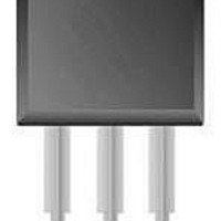
... DS see Figure 13 Simplified outline SOT78A (TO-220AB) Description plastic single-ended package; heatsink mounted; 1 mounting hole; 3-lead TO-220AB All information provided in this document is subject to legal disclaimers. Rev. 2 — 2 February 2011 BUK7526-100B N-channel TrenchMOS standard level FET Min ≤ 100 V; - sup = °C; j Graphic symbol ...
Page 3
... P der (%) 150 200 ( ° Fig 2. Normalized total power dissipation as a function of mounting base temperature All information provided in this document is subject to legal disclaimers. Rev. 2 — 2 February 2011 BUK7526-100B N-channel TrenchMOS standard level FET Min - - -20 - Figure 1 - ≤ 10 µ -55 - ° Ω; - ...
Page 4
... Transient thermal impedance from junction to mounting base as a function of pulse duration BUK7526-100B Product data sheet = DSon Conditions see Figure 4 −5 −4 − All information provided in this document is subject to legal disclaimers. Rev. 2 — 2 February 2011 BUK7526-100B N-channel TrenchMOS standard level FET 03nm43 = 10 μ 100 μ 100 (V) DS Min Typ - - ...
Page 5
... °C j from source lead 6 mm from package to source bond pad ° ° see Figure /dt = -100 A/µ - ° All information provided in this document is subject to legal disclaimers. Rev. 2 — 2 February 2011 BUK7526-100B Min Typ Max Unit 100 - - 4 500 µA - 0.02 1 µ ...
Page 6
... R 8 7.5 7 6.5 6 5 (V) DS Fig 6. 03aa35 typ max (V) GS Fig 8. All information provided in this document is subject to legal disclaimers. Rev. 2 — 2 February 2011 BUK7526-100B N-channel TrenchMOS standard level FET 50 DSon (mΩ Drain-source on-state resistance as a function of gate-source voltage; typical values ( Forward transconductance as a function of drain current ...
Page 7
... Fig 10. Gate-source threshold voltage as a function of 03nm41 Label 100 I (A) D Fig 12. Normalized drain-source on-state resistance All information provided in this document is subject to legal disclaimers. Rev. 2 — 2 February 2011 BUK7526-100B N-channel TrenchMOS standard level FET 5 GS(th) (V) 4 max 3 typ 2 min 1 0 − junction temperature 2 ...
Page 8
... Fig 14. Input, output and reverse transfer capacitances 100 °C = 175 ° 0.0 0.5 1.0 All information provided in this document is subject to legal disclaimers. Rev. 2 — 2 February 2011 BUK7526-100B N-channel TrenchMOS standard level FET C iss C oss C rss 0 −2 − function of drain-source voltage; typical values 03nm35 1.5 V ...
Page 9
... 0.7 15.8 6.4 10.3 2.54 0.4 15.2 5.9 9.7 REFERENCES JEDEC JEITA 3-lead TO-220AB SC-46 All information provided in this document is subject to legal disclaimers. Rev. 2 — 2 February 2011 BUK7526-100B N-channel TrenchMOS standard level FET mounting base ( max. 15.0 3.30 3.8 3.0 3.0 13 ...
Page 10
... The format of this data sheet has been redesigned to comply with the new identity guidelines of NXP Semiconductors. • Legal texts have been adapted to the new company name where appropriate. • Type number BUK7526-100B separated from data sheet BUK75_7626_100B-01. BUK75_7626_100B-01 20030411 (9397 750 11238) BUK7526-100B ...
Page 11
... In case an individual All information provided in this document is subject to legal disclaimers. Rev. 2 — 2 February 2011 BUK7526-100B N-channel TrenchMOS standard level FET © NXP B.V. 2011. All rights reserved ...
Page 12
... TrenchMOS, TriMedia and UCODE — are trademarks of NXP B.V. HD Radio and HD Radio logo — are trademarks of iBiquity Digital Corporation. http://www.nxp.com salesaddresses@nxp.com All information provided in this document is subject to legal disclaimers. Rev. 2 — 2 February 2011 BUK7526-100B N-channel TrenchMOS standard level FET Trademarks © NXP B.V. 2011. All rights reserved ...
Page 13
... Please be aware that important notices concerning this document and the product(s) described herein, have been included in section ‘Legal information’. © NXP B.V. 2011. For more information, please visit: http://www.nxp.com For sales office addresses, please send an email to: salesaddresses@nxp.com All rights reserved. Date of release: 2 February 2011 Document identifier: BUK7526-100B ...