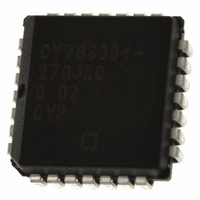
CY7B9334-270JXC Cypress Semiconductor Corp, CY7B9334-270JXC Datasheet - Page 4

CY7B9334-270JXC
Manufacturer Part Number
CY7B9334-270JXC
Description
IC RECEIVER HOTLINK 28-PLCC
Manufacturer
Cypress Semiconductor Corp
Series
HOTlink™r
Type
Transmitter and Receiverr
Datasheet
1.CY7B9234-270JXC.pdf
(36 pages)
Specifications of CY7B9334-270JXC
Package / Case
28-PLCC
Protocol
Fibre Channel
Voltage - Supply
4.5V ~ 5.5V
Mounting Type
Surface Mount
Product
PHY
Supply Voltage (min)
4.5 V
Supply Current
0.155 A
Maximum Operating Temperature
+ 70 C
Minimum Operating Temperature
0 C
Mounting Style
SMD/SMT
Number Of Channels
1
Lead Free Status / RoHS Status
Lead free / RoHS Compliant
Number Of Drivers/receivers
-
Lead Free Status / RoHS Status
Lead free / RoHS Compliant, Lead free / RoHS Compliant
Other names
428-2908-5
CY7B9334-270JXC
CY7B9334-270JXC
Available stocks
Company
Part Number
Manufacturer
Quantity
Price
Company:
Part Number:
CY7B9334-270JXC
Manufacturer:
CYPRESS
Quantity:
831
Company:
Part Number:
CY7B9334-270JXC
Manufacturer:
Cypress Semiconductor Corp
Quantity:
10 000
Company:
Part Number:
CY7B9334-270JXCT
Manufacturer:
Cypress Semiconductor Corp
Quantity:
10 000
Pin Description
CY7B9234 SMPTE HOTLink Transmitter (continued)
Document #: 38-02014 Rev. *B
ENN
CKW
FOTO
OUT A±
OUT B±
OUT C±
MODE
BISTEN
RP
V
V
GND
Name
CCN
CCQ
TTL In
TTL In
TTL In
PECL Out Differential Serial Data Outputs. These PECL 100K outputs (+5V referenced) are capable of driving
3-Level In
TTL In
TTL Out
I/O
Enable Next Parallel Data. If ENN is LOW, the data appearing on D
CKW is loaded, encoded, and sent. If ENA and ENN are HIGH, the data appearing on D
next rising edge of CKW will be ignored and the Transmitter will insert a Null character to fill the space
between user data. ENN may be held HIGH/LOW continuously or it may be pulsed with each data
byte sent. If ENN is being used for data control, ENA will normally be strapped HIGH, but can be used
for BIST function control.
Clock Write. CKW is both the clock frequency reference for the multiplying PLL that generates the
high-speed transmit clock, and the byte rate write signal that synchronizes the parallel data input.
CKW must be connected to a crystal controlled time base that runs within the specified frequency
range of the Transmitter and Receiver.
Fiber-Optic Transmitter Off. FOTO determines the function of two of the three PECL transmitter
output pairs. If FOTO is LOW, the data encoded by the Transmitter will appear at the outputs contin-
uously. If FOTO is HIGH, OUTA± and OUTB± are forced to their “logic zero” state (OUT+ = LOW and
OUT− = HIGH), causing a fiber-optic transmit module to extinguish its light output. OUTC is unaffected
by the level on FOTO, and can be used as a loop-back signal source for board-level diagnostic testing.
terminated transmission lines or commercial fiber-optic transmitter modules. Unused pairs of outputs
can be wired to V
level on FOTO, and will remain at their “logical zero” states when FOTO is asserted. OUTC± is unaffected by
the level on FOTO (OUTA+ and OUTB+ are used as a differential test clock input while in Test mode, i.e.,
MODE=UNCONNECTED or forced to V
Encoder Mode Select. The level on MODE determines the encoding method to be used. When wired
to GND, MODE selects 8B/10B encoding. When wired to V
bit pattern on D
internal bit-clock generator is disabled and OUTA+/OUTB+ become the differential bit clock to be used for
factory test. In typical applications MODE is wired to V
Built-In Self-Test Enable. When BISTEN is LOW and ENA and ENN are HIGH, the transmitter sends an
alternating 1−0 pattern (D10.2 or D21.5). When either ENA or ENN is set LOW and BISTEN is LOW, the
transmitter begins a repeating test sequence that allows the Transmitter and Receiver to work together to test
the function of the entire link. In normal use this input is held HIGH or wired to V
free-running pattern generator that need not be initialized, but if required, the BIST sequence can be initialized
by momentarily asserting SVS while BISTEN is LOW. BISTEN has the same timing as D
Read Pulse. RP is a 60% LOW duty-cycle byte-rate pulse train suitable for the read pulse in CY7C42X
FIFOs. The frequency on RP is the same as CKW when enabled by ENA, and duty cycle is independent of
the CKW duty cycle. Pulse widths are set by logic internal to the transmitter. In BIST mode, RP will remain
HIGH for all but the last byte of a test loop. RP will pulse LOW one byte time per BIST loop.
Power for output drivers.
Power for internal circuitry.
Ground.
Description
a–j
goes directly to the shifter. When left floating (internal resistors hold the input at V
CC
to reduce power if the output is not required. OUTA± and OUTB± are controlled by the
CC
/2).
CC
or GND.
CC
, data inputs bypass the encoder and the
0−7
at the next rising edge of
CC
. The BIST generator is a
0−7
.
CY7B9234
CY7B9334
0−7
CC
Page 4 of 36
at the
/2) the
[+] Feedback


