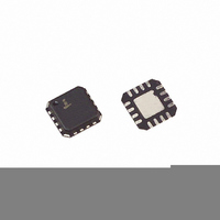
EL1511CLZ Intersil, EL1511CLZ Datasheet - Page 14

EL1511CLZ
Manufacturer Part Number
EL1511CLZ
Description
IC LINE DRIVER ADSL/VDSL 16-QFN
Manufacturer
Intersil
Type
Driverr
Datasheet
1.EL1511CL.pdf
(18 pages)
Specifications of EL1511CLZ
Number Of Drivers/receivers
1/0
Protocol
DSL
Voltage - Supply
5 V ~ 15 V
Mounting Type
Surface Mount
Package / Case
16-VQFN Exposed Pad, 16-HVQFN, 16-SQFN, 16-DHVQFN
Lead Free Status / RoHS Status
Lead free / RoHS Compliant
Available stocks
Company
Part Number
Manufacturer
Quantity
Price
Part Number:
EL1511CLZ
Manufacturer:
INTERSIL
Quantity:
20 000
Applications Information
Product Description
The EL1511 is a dual operational amplifier designed for
customer premise driver functions in DMT ADSL solutions
and is built using Elantec's proprietary complimentary bipolar
process. Due to the current feedback architecture, the
EL1511 closed-loop 3dB bandwidth is dependent on the
value of the feedback resistor. First the desired bandwidth is
selected by choosing the feedback resistor, R
gain is set by picking the gain resistor, R
beginning of the Typical Performance Curves section show
the effect of varying both R
Power Supply Bypassing and Printed Circuit
Board Layout
As with any high frequency device, good printed circuit
board layout is necessary for optimum performance. Ground
plane construction is highly recommended. Lead lengths
should be as short as possible, below ¼. The power supply
pins must be well bypassed to reduce the risk of oscillation.
A 1.0µF tantalum capacitor in parallel with a 0.01µF ceramic
capacitor is adequate for each supply pin.
For good AC performance, parasitic capacitances should be
kept to a minimum, especially at the inverting input (see
Capacitance at the Inverting Input section). This implies
keeping the ground plane away from this pin. Carbon resistors
are acceptable, while use of wire-wound resistors should not
be used because of their parasitic inductance. Similarly,
capacitors should be low inductance for best performance.
Use of sockets, particularly for the SO (0.150") package,
should be avoided. Sockets add parasitic inductance and
capacitance which will result in peaking and overshoot.
Capacitance at the Inverting Input
Due to the topology of the current feedback amplifier, stray
capacitance at the inverting input will affect the AC and
transient performance of the EL1511 when operating in the
non-inverting configuration.
In the inverting gain mode, added capacitance at the inverting
input has little effect since this point is at a virtual ground and
stray capacitance is therefore not “seen” by the amplifier.
Feedback Resistor Values
The EL1511 has been designed and specified with R
1.5kΩ for A
relatively flat frequency response with <1.5dB peaking out to
60MHz. As is the case with all current feedback amplifiers,
wider bandwidth, at the expense of slight peaking, can be
obtained by reducing the value of the feedback resistor.
Inversely, larger values of feedback resistor will cause rolloff
to occur at a lower frequency. By reducing R
bandwidth can be extended to 70MHz with 3.0dB of peaking.
See the curves in the Typical Performance Curves section
which show 3dB bandwidth and peaking vs frequency for
various feedback resistors.
V
= +5. This value of feedback resistor yields
F
14
and R
G
.
G
. The curves at the
F
F
, and then the
to 1kΩ,
F
=
EL1511
PD
PD
Power Dissipation
The EL1511 amplifier combines both high speed and large
output current drive capability at a moderate supply current
in very small packages. It is possible to exceed the
maximum junction temperature allowed under certain supply
voltage, temperature, and loading conditions. To ensure that
the EL1511 remains within its absolute maximum ratings, the
following discussion will help to avoid exceeding the
maximum junction temperature.
The maximum power dissipation allowed in a package is
determined by its thermal resistance and the amount of
temperature rise according to:
P
The maximum power dissipation actually produced by an IC
is the total quiescent supply current times the total power
supply voltage plus the power in the IC due to the load, or:
where I
quiescent supply current flowing in the output driver transistor
should be subtracted from the first term because, under
loading and due to the class AB nature of the output stage,
the output driver current is now included in the second term.)
In general, an amplifier's AC performance degrades at
higher operating temperature and lower supply current.
Unlike some amplifiers, the EL1511 maintains almost
constant supply current over temperature so that AC
performance is not degraded as much over the entire
operating temperature range.
Estimating Line Driver Power Dissipation in ADSL
CPE Application
The below figure shows a typical ADSL CPE line driver
implementation. The average line power requirement for the
ADSL CPE application is 13dBM (20mW) into a 100W line.
The average line voltage is 1.41V
to average ratio (crest factor) of 5.3 implies peak voltage of
7.5V into the line. Using a differential drive configuration and
transformer coupling with standard back termination, a
transformer ratio of 1:2 is selected. With 1:2 transformer
ratio, the impedance across the driver side of the
transformer is 25Ω, the average voltage is 0.705V
the average current is 28.2mA. The power dissipated in the
EL1511 is a combination of the quiescent power and the
output stage power when driving the line:
In the ½ power mode, the EL1511 consumes typically 6.6mA
quiescent current and still able to maintain very low
distortion. The distortion results are shown in typical
P
DMAX
DMAX
=
=
P
V
S
quiescent
S
=
=
×
is the supply current. (To be more accurate, the
T
-------------------------------------------- -
2
I
Q
JMAX
×
+
V
(
S
V
θ
+
+
–
S
JA
P
(
T
–
V
output-stage
AMAX
2
S
×
–
V
V
OUT-RMS
OUT
)
×
V
--------------- -
RMS
OUT
R
)
L
×
I
. The ADSL DMT peak
OUT-RMS
RMA
April 10, 2007
FN7016.2
and


