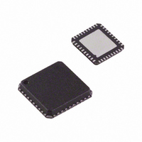
ADV7393BCPZ Analog Devices Inc, ADV7393BCPZ Datasheet - Page 79

ADV7393BCPZ
Manufacturer Part Number
ADV7393BCPZ
Description
IC DAC VIDEO HDTV 10BIT 40LFCSP
Manufacturer
Analog Devices Inc
Type
Video Encoderr
Datasheet
1.ADV7393BCPZ.pdf
(108 pages)
Specifications of ADV7393BCPZ
Design Resources
Reconstruction Video Filter Using ADA4430-1 Amplifier After ADV7393 Video Encoder (CN0101)
Applications
Set-Top Boxes, Video Players, Displays
Voltage - Supply, Analog
2.6 V ~ 3.46 V
Voltage - Supply, Digital
1.71 V ~ 1.89 V
Mounting Type
Surface Mount
Package / Case
40-LFCSP
Input Format
Digital
Output Format
Analog
Supply Voltage Range
1.71V To 1.89V
Operating Temperature Range
-40°C To +85°C
Tv / Video Case Style
LFCSP
No. Of Pins
40
Msl
MSL 1 - Unlimited
Lead Free Status / RoHS Status
Lead free / RoHS Compliant
For Use With
ADV7393-DBRDZ - BOARD EVAL FOR ADV7393EVAL-ADV7393EBZ - BOARD EVAL FOR ADV7393 ENCODER
Lead Free Status / RoHS Status
Lead free / RoHS Compliant, Lead free / RoHS Compliant
Available stocks
Company
Part Number
Manufacturer
Quantity
Price
Company:
Part Number:
ADV7393BCPZ
Manufacturer:
SIEMENS
Quantity:
101
Part Number:
ADV7393BCPZ
Manufacturer:
ADI/亚德诺
Quantity:
20 000
Company:
Part Number:
ADV7393BCPZ-3
Manufacturer:
ADI
Quantity:
302
Part Number:
ADV7393BCPZ-3
Manufacturer:
ADI/亚德诺
Quantity:
20 000
Company:
Part Number:
ADV7393BCPZ3
Manufacturer:
OSRAM
Quantity:
4 298
INTERNAL TEST PATTERN GENERATION
SD TEST PATTERNS
The ADV739x is able to internally generate SD color bar and
black bar test patterns. For this function, a 27 MHz clock signal
must be applied to the CLKIN pin.
The register settings in Table 61 are used to generate an SD NTSC
75% color bar test pattern. All other registers are set as normal/
default. Component YPrPb output is available on DAC 1 to
DAC 3. On power-up, the subcarrier frequency registers default
to the appropriate values for NTSC.
Table 61. SD NTSC Color Bar Test Pattern Register Writes
Subaddress
0x00
0x82
0x84
For CVBS and S-Video (Y/C) output, 0xCB instead of 0xC9
should be written to Subaddress 0x82.
For component RGB output rather than YPrPb output, 0 should
be written to Subaddress 0x02, Bit 5.
To generate an SD NTSC black bar test pattern, the settings
shown in Table 61 should be used with an additional write of
0x24 to Subaddress 0x02.
For PAL output of either test pattern, the same settings are used
except that Subaddress 0x80 is programmed to 0x11, and the
subcarrier frequency (F
in Table 62.
Table 62. PAL F
Subaddress
0x8C
0x8D
0x8E
0x8F
Note that, when programming the F
write the values in the sequence F
F
complete.
SC
value to be written is only accepted after the F
SC
Register Writes
SC
Description
F
F
F
F
) registers are programmed as shown
SC
SC
SC
SC
0
1
2
3
SC
0, F
SC
registers, the user must
SC
Setting
0x1C
0xC9
0x40
1, F
SC
2, F
SC
Setting
0xCB
0x8A
0x09
0x2A
SC
3 write is
3. The full
Rev. B | Page 79 of 108
ED/HD TEST PATTERNS
The ADV739x is able to internally generate ED/HD color bar,
black bar, and hatch test patterns. For ED test patterns, a 27 MHz
clock signal must be applied to the CLKIN pin. For HD test
patterns, a 74.25 MHz clock signal must be applied to the
CLKIN pin.
The register settings in Table 63 are used to generate an ED
525p hatch test pattern. All other registers are set as normal/
default. Component YPrPb output is available on DAC 1 to
DAC 3. For component RGB output rather than YPrPb output,
0 should be written to Subaddress 0x02, Bit 5.
Table 63. ED 525p Hatch Test Pattern Register Writes
Subaddress
0x00
0x01
0x31
To generate an ED 525p black bar test pattern, the settings
shown in Table 63 should be used with an additional write of
0x24 to Subaddress 0x02.
To generate an ED 525p flat field test pattern, the settings
shown in Table 63 should be used, except that 0x0D should be
written to Subaddress 0x31.
The Y, Cr, and Cb levels for the hatch and flat field test patterns
can be controlled using Subaddress 0x36, Subaddress 0x37, and
Subaddress 0x38, respectively.
For ED/HD standards other than 525p, the settings shown in
Table 63 (and subsequent comments) are used, except that
Subaddress 0x30, Bits[7:3] are updated as appropriate.
ADV7390/ADV7391/ADV7392/ADV7393
Setting
0x1C
0x10
0x05


