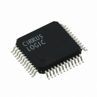
CS4954-CQZ Cirrus Logic Inc, CS4954-CQZ Datasheet - Page 33

CS4954-CQZ
Manufacturer Part Number
CS4954-CQZ
Description
IC VIDEO ENCODER NTSC/PAL 48TQFP
Manufacturer
Cirrus Logic Inc
Type
Video Encoderr
Datasheet
1.CS4954-CQZ.pdf
(60 pages)
Specifications of CS4954-CQZ
Package / Case
48-TQFP, 48-VQFP
Voltage - Supply, Analog
3.15 V ~ 5.25 V
Voltage - Supply, Digital
3.15 V ~ 5.25 V
Mounting Type
Surface Mount
Operating Supply Voltage
3.3 V / 5 V
Supply Current
70 mA
Maximum Operating Temperature
+ 85 C
Minimum Operating Temperature
- 40 C
Mounting Style
SMD/SMT
Number Of Channels
2
Resolution
10 bit
Snr
70 dB
Input Format
Digital
Output Format
Analog
Supply Voltage Range
3.15V To 3.45V
Operating Temperature Range
-40°C To +85°C
Tv / Video Case Style
TQFP
No. Of Pins
48
Tv / Video Type
Encoder
Rohs Compliant
Yes
Filter Terminals
SMD
Lead Free Status / RoHS Status
Lead free / RoHS Compliant
For Use With
CDB4955A - EVALUATION BOARD FOR CS4955A
Applications
-
Lead Free Status / Rohs Status
Lead free / RoHS Compliant
Other names
598-1682
Available stocks
Company
Part Number
Manufacturer
Quantity
Price
Part Number:
CS4954-CQZ
Manufacturer:
CIRRUS
Quantity:
20 000
Company:
Part Number:
CS4954-CQZR
Manufacturer:
NXP
Quantity:
11 000
Company:
Part Number:
CS4954-CQZR
Manufacturer:
Cirrus Logic Inc
Quantity:
10 000
Part Number:
CS4954-CQZR
Manufacturer:
CIRRUS
Quantity:
20 000
7.4.2 Chrominance DAC
The C output pin is driven from a 10-bit 27 MHz
current output DAC that internally receives the C
or chrominance portion of the video signal (color
only). The C DAC is designed to drive proper video
levels into a 37.5 Ω load. Reference the detailed
electrical section of this data sheet for the exact C
digital to analog AC and DC performance data. The
EN_C enable control register bit in Control Register
1 (0×05) is provided to enable or disable the
chrominance DAC. To completely disable or for
low power device operation, the chrominance DAC
can be totally shut down via the SVIDCHR_PD
register bit in Control Register 4 (0×04). In this
mode turn-on using the control register will not be
instantaneous.
7.4.3 CVBS DAC
The CVBS output pin is driven from a 10-bit
27 MHz current output DAC that internally re-
ceives a combined luma and chroma signal to pro-
vide composite video output. The CVBS DAC is
designed to drive proper composite video levels
into a 37.5 Ω load. Reference the detailed electrical
section of this data sheet for the exact CVBS digital
to analog AC and DC performance data. The
EN_COM enable control register bit, in Control
Register 1 (0×05), is provided to enable or disable
the output pin. When disabled, there is no current
flow from the output. To completely disable or for
low power device operation, the CVBS37 DAC can
be totally shut down via the COMDAC_PD control
register bit in Control Register 4 (0×04). In this
mode turn-on using the control register will not be
instantaneous.
7.4.4 Red DAC
The Red output pin is driven from a 10-bit 27 MHz
current output DAC that internally receives either
red component video data or V (Cr) data. The Red
DAC is designed to drive proper component video
levels into a 37.5 Ω load. Reference the detailed
DS278F6
electrical section of this data sheet for the exact red
digital to analog AC and DC performance data. The
EN_R enable control register bit in Control Regis-
ter 1 (0×05) is provided to enable or disable the out-
put pin. When disabled, there is no current flow
from the output. To complete disable or for low
power device operation, the red DAC can be totally
shut down via the R_PD control register bit in
Control Register 4 (0×04). In this mode turn-on
using the control register will not be instantaneous.
7.4.5 Green DAC
The Green output pin is driven from a 10-bit
27 MHz current output DAC that internally re-
ceives either Green component video data, Y lumi-
nance data or CVBS data depending upon its
configuration. See
page 33
The Green DAC is designed to drive proper com-
posite video levels into a 37.5 Ω load. Reference
the detailed electrical section of this data sheet for
the exact green digital to analog AC and DC perfor-
mance data. The EN_G enable control register bit,
in Control Register 1 (0×05), is provided to enable
or disable the output pin. When disabled, there is
no current flow from the output. To completely dis-
able or for low power device operation, the green
DAC can be totally shut down via the G_PD con-
trol register bit in Control Register 4
mode turn-on using the control register will not be
instantaneous.
7.4.6 Blue DAC
The Blue output pin is driven from a 10-bit 27 MHz
current output DAC that internally receives either
blue component video data or U (Cb) data. The
Blue DAC is designed to drive proper component
video levels into a 37.5 Ω load. Reference the de-
tailed electrical section of this data sheet for the ex-
act blue digital to analog AC and DC performance
data. The EN_B enable control register bit, in Con-
trol Register 5 (0×05), is provided to enable or dis-
able the output pin. When disabled, there is no
and
“Luminance DAC” on page
Table
CS4954 CS4955
1,
“CVBS DAC” on
(0×04).
In this
32.
33


