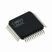
CS4954-CQZ Cirrus Logic Inc, CS4954-CQZ Datasheet - Page 53

CS4954-CQZ
Manufacturer Part Number
CS4954-CQZ
Description
IC VIDEO ENCODER NTSC/PAL 48TQFP
Manufacturer
Cirrus Logic Inc
Type
Video Encoderr
Datasheet
1.CS4954-CQZ.pdf
(60 pages)
Specifications of CS4954-CQZ
Package / Case
48-TQFP, 48-VQFP
Voltage - Supply, Analog
3.15 V ~ 5.25 V
Voltage - Supply, Digital
3.15 V ~ 5.25 V
Mounting Type
Surface Mount
Operating Supply Voltage
3.3 V / 5 V
Supply Current
70 mA
Maximum Operating Temperature
+ 85 C
Minimum Operating Temperature
- 40 C
Mounting Style
SMD/SMT
Number Of Channels
2
Resolution
10 bit
Snr
70 dB
Input Format
Digital
Output Format
Analog
Supply Voltage Range
3.15V To 3.45V
Operating Temperature Range
-40°C To +85°C
Tv / Video Case Style
TQFP
No. Of Pins
48
Tv / Video Type
Encoder
Rohs Compliant
Yes
Filter Terminals
SMD
Lead Free Status / RoHS Status
Lead free / RoHS Compliant
For Use With
CDB4955A - EVALUATION BOARD FOR CS4955A
Applications
-
Lead Free Status / Rohs Status
Lead free / RoHS Compliant
Other names
598-1682
Available stocks
Company
Part Number
Manufacturer
Quantity
Price
Part Number:
CS4954-CQZ
Manufacturer:
CIRRUS
Quantity:
20 000
Company:
Part Number:
CS4954-CQZR
Manufacturer:
NXP
Quantity:
11 000
Company:
Part Number:
CS4954-CQZR
Manufacturer:
Cirrus Logic Inc
Quantity:
10 000
Part Number:
CS4954-CQZR
Manufacturer:
CIRRUS
Quantity:
20 000
9.
The printed circuit layout should be optimized for
lowest noise on the CS4954/5 placed as close to the
output connectors as possible. All analog supply
traces should be as short as possible to minimize in-
ductive ringing.
A well designed power distribution network is es-
sential in eliminating digital switching noise. The
ground planes must provide a low-impedance re-
turn path for the digital circuits. A PC board with a
minimun of four layers is recommended. The
ground layer should be used as a shield to isolate
noise from the analog traces. The top layer (1)
should be reserved for analog traces but digital
traces can share this layer if the digital signals have
sufficiently slow edges and edge rates and switch
little current or if they are separated from the ana-
log traces by a signigicant distance (dependent on
their frequency content and current). The PCB lay-
er “stack up” (from top to bottom) should be: ana-
log/digital signal then ground plane followed by
the analog power plane and the digital signal layer.
9.1
The power and ground planes need isolation gaps
of at least 0.05" to minimize digital switching noise
effects on the analog signals and components. A
split analog/digital ground plane should be con-
nected at one location as close as possible to the
CS4954/5.
9.2
Start by reducing power supply ripple and wiring
harness inductance by placing a large (33-100 uF)
capacitor as close to the power entry point as pos-
sible. Use separate power planes or traces for the
digital and analog sections even if they use the
same supply. If necessary, further isolate the digital
and analog power supplies by using ferrite beads on
each supply branch followed by a low ESR capac-
itor.
DS278F6
BOARD DESIGN AND LAYOUT
CONSIDERATIONS
Power and Ground Planes
Power Supply Decoupling
Place all decoupling caps as close as possible to the
device. Surface mount capacitors generally have
lower inductance than radial lead or axial lead com-
ponents. Surface mount caps should be place on the
component side of the PCB to minimize inductance
caused by board vias. Any vias, especially to
ground, should be as large as possible to reduce
their inductive effects.
9.3
The digital inputs and outputs of the CS4954/5
should be isolated from the analog outputs as much
as possible. Use separate signal layers whenever
possible and do not route digital signals over the
analog power and ground planes.
Noise from the digital section is related to the digi-
tal edge rates and rise/fall times. Ringing, over-
shoot, undershoot, and ground bounce are all
related to edge rise/fall times. Use lower speed log-
ic such as HCMOS for the host port interface to re-
duce switching noise. For the video input ports,
higher speed logic is required, but use logic that
produces the slowest practical edge rise/fall times
to reduce noise. It is also important to match the
source impedance, line impedance, and load im-
pedance as much as possible. Generally, if the line
length is greater than one fourth of the signal wave-
length or period (from λ = ν/f), a line termination is
necessary. Ringing can also be reduced by damping
the line with a series resistor (22-150 Ω). Under ex-
treme cases, it may be advisable to use microstrip
techniques to further reduce radiated switching
noise if there are very fast (<2 ns) rise/fall times in
the system. If microstrip techniques are used, split
the analog and digital ground planes and use proper
RF decoupling techniques.
9.4
The CS4954/5 should be located as close as possi-
ble the output connectors to minimize noise pickup
and reflections due to impedance mismatch. All un-
used analog outputs should be placed in shutdown.
Digital Interconnect
Analog Interconnect
CS4954 CS4955
53


