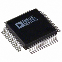
ADV7195KS Analog Devices Inc, ADV7195KS Datasheet - Page 10

ADV7195KS
Manufacturer Part Number
ADV7195KS
Description
IC DAC VID-HDTV 3CH-11BIT 52MQFP
Manufacturer
Analog Devices Inc
Type
Video Encoderr
Datasheet
1.ADV7195KS.pdf
(36 pages)
Specifications of ADV7195KS
Rohs Status
RoHS non-compliant
Applications
HDTV, MPEG, Image Processing
Voltage - Supply, Analog
3.3V
Voltage - Supply, Digital
3.3V
Mounting Type
Surface Mount
Package / Case
52-MQFP, 52-PQFP
Adc/dac Resolution
11b
Screening Level
Commercial
Package Type
MQFP
Pin Count
52
For Use With
EVAL-ADV7195EB - BOARD EVAL FOR ADV7195
Lead Free Status / RoHS Status
Not Compliant
Available stocks
Company
Part Number
Manufacturer
Quantity
Price
Part Number:
ADV7195KSZ
Manufacturer:
ADI/亚德诺
Quantity:
20 000
ADV7195
FUNCTIONAL DESCRIPTION
Digital Inputs
The digital inputs of the ADV7195 are TTL-compatible. 30-bit
YCrCb or RGB pixel data in 4:4:4 format or 20-bit YCrCb
pixel data in 4:2:2 format is latched into the device on the rising
edge of each clock cycle at 27 MHz in Progressive Scan Mode or
74.25 MHz or 74.1785 MHz in HDTV mode. It is also possible
to input 3 × bit RGB data in 4:4:4 format to the ADV7195. It
is recommended to input data in 4:2:2 mode to make use of the
chroma SSAFs on the ADV7195. As can be seen in Figures 6 and
7, this filter has 0 dB passband response and prevents signal com-
ponents being loaded back into the frequency band. In 4:4:4 input
mode, the video data is already interpolated by the external
input device and the chroma SSAFs of the ADV7195 are bypassed.
ATTEN
RL –10.0dBm
START 100kHz
ATTEN
RL –10.0dBm
START 100kHz
RBW 10kHz
RBW 10kHz
10dB
10dB
VBW 300Hz
VBW
VAVG
VAVG
10dB/
10dB/
1
4
300Hz
3.18MHz
3.12MHz
STOP
STOP
MKR
MKR
–3.00dB
20.00MHz
0dB
20.00MHz
SWP
SWP 17.0SEC
17.0SEC
Control Signals
The ADV7195 accepts sync control signals accompanied by
valid 4:2:2 or 4:4:4 data. These external horizontal, vertical, and
blanking pulses (or EAV/SAV codes) control the insertion of
appropriate sync information into the output signals.
Analog Outputs
The analog Y signal is output on the 11-bit + Sync DAC A,
the color component analog signals on the 11-bit DAC B and
DAC C conforming to EIA-770.1 or EIA-770.2 standards in PS
mode or EIA-770.3 in HDTV mode. R
(EIA-770.1, EIA-770.2, EIA-770.3), R
For RGB outputs conforming to RS-170/RS-343A output stan-
dards R
Undershoot Limiter
A limiter can be applied to the Y data before it is applied to the
DACs. Available limit values are –1.5 IRE, –6 IRE, –11 IRE below
blanking. This functionality is available in Progressive Scan
Mode only.
I
A selectable internal I
on the I
on the I
passed to the I
input bandwidth on the I
Internal Test Pattern Generator
The ADV7195 can generate a crosshatch pattern (white lines
against a black background). Additionally, the ADV7195 can
output a uniform color pattern. The color of the lines or uni-
form field/frame can be programmed by the user.
Y/CrCb Delay
The Y output and the color component outputs can be delayed
wrt the falling edge of the horizontal sync signal by up to four
clock cycles.
Gamma Correction
Gamma correction may be performed on the luma data. The
user has the choice to use either of two different gamma curves,
A or B. At any one time one of these curves is operational if
gamma correction is enabled. Gamma correction allows the
mapping of the luma data to a user-defined function.
54 MHz Operation
In Progressive Scan mode, it is possible to operate the three
output DACs at 54 MHz or 27 MHz. The ADV7195 is sup-
plied with a 27 MHz clock synced with the incoming data. If
required, a second stage interpolation filter interpolates the data
to 54 MHz before it is applied to the three output DACs.
The second stage interpolation filter is controlled by MR36. After
applying a Reset, it is recommended to toggle this bit. Before
toggling this bit, 3Ehex must be written to Address 09hex.
PROGRAMMABLE SHARPNESS FILTER
Sharpness Filter Mode is applicable to the Y data only in
Progressive Scan Mode.
The desired frequency response can be chosen by the user in
programming the correct value via the I
frequency responses can be seen in the figures on the follow-
ing pages.
2
C Filter
SET
2
2
C lines is reduced and pulses of less than 50 ns are not
C interface. In setting ALSB high, the input bandwidth
must have a value of 2820 Ω.
2
C controller. Setting ALSB low allows greater
2
C filter allows significant noise reductions
2
C lines.
LOAD
SET
2
C. The variation of
has a value of 2470 Ω
has a value of 300 Ω.


