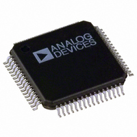
ADV7303AKST Analog Devices Inc, ADV7303AKST Datasheet - Page 29

ADV7303AKST
Manufacturer Part Number
ADV7303AKST
Description
IC DAC VIDEO HDTV 6-11BIT 64LQFP
Manufacturer
Analog Devices Inc
Type
Video Encoderr
Datasheet
1.ADV7303AKST.pdf
(68 pages)
Specifications of ADV7303AKST
Rohs Status
RoHS non-compliant
Applications
DVD, Set-Top Boxes
Voltage - Supply, Analog
2.37 V ~ 2.63 V
Voltage - Supply, Digital
2.37 V ~ 3.6 V
Mounting Type
Surface Mount
Package / Case
64-LQFP
Number Of Dac's
6
Adc/dac Resolution
11b
Screening Level
Commercial
Package Type
LQFP
Pin Count
64
Lead Free Status / RoHS Status
Compliant
Available stocks
Company
Part Number
Manufacturer
Quantity
Price
INPUT AND OUTPUT CONFIGURATION
STANDARD DEFINITION ONLY
The 8-bit multiplexed input data is input on Pins S7–S0, with S0
being the LSB. ITU-R.BT601/ITU-R.BT656 input standards
are supported. In 16-bit Input Mode, the Y pixel data is input on
Pins S7–S0 and CrCb data on Pins Y7–Y0. The 27 MHz clock
input must be input on Pin CLKIN_A. Input sync signals are
optional and are input on the S_VSYNC, S_HSYNC, and
S_BLANK pins.
PROGRESSIVE SCAN ONLY OR HDTV ONLY
YCrCb Progressive Scan, HDTV, or any other HD YCrCb data
can be input in 4:2:2 or 4:4:4 format. In 4:2:2 Input Mode, the
Y data is input on Pins Y7–Y0 and the CrCb data on Pins C7–
C0. In 4:4:4 Input Mode, Y data is input on Pins Y7–Y0, Cb
data on Pins C7–C0, and Cr data on Pins S7–S0. If the
YCrCb data does not conform to SMPTE293M (525 p),
ITU-R.BT1358M (625 p), SMPTE274M (1080 i),
SMPTE296M (720 p), or BTA-T1004, the Async Timing Mode
must be used. RGB data can only be input in 4:4:4 format in
PS Input Mode only, or HDTV Input Mode only, when HD
RGB input is enabled. G data is input on Pins Y7–Y0, R data
on S7–S0, and B data on Pins C7–C0. The clock signal must
be input on Pin CLKIN_A. Synchronization signals are optional
and are input on Pins P_VSYNC, P_HSYNC, and P_BLANK.
SIMULTANEOUS STANDARD DEFINITION AND
PROGRESSIVE SCAN OR HDTV
YCrCb PS, HDTV, or any other HD data must be input in 4:2:2
format. In 4:2:2 Input Mode, the Y data is input on Pins Y7–Y0
and the CrCb data on C7–C0. If PS 4:2:2 data is interleaved onto a
single 8-bit bus, Pins Y7–Y0 are used for the input port. The inter-
leaved data is to be input at 27 MHz in setting the Input Mode
Register at Address 01h accordingly. If the YCrCb data does not
conform to SMPTE293M (525 p), ITU-R.BT1358M (625 p),
REV. A
Figure 20. Standard Definition Only Input Mode
Figure 21. Progressive Scan Only Input Mode
DECODER
PROGRESSIVE
INTERLACED
MPEG2
DECODER
YCrCb
MPEG2
TO
YCrCb
27MHz
27MHz
Cr
Cb
Y
3
8
8
8
8
3
S_VSYNC
S_HSYNC
S_BLANK
CLKIN_A
S7–S0
ADV7302A/
ADV7303A
CLKIN_A
S7–S0
C7–C0
Y7–Y0
P_VSYNC
P_HSYNC
P_BLANK
ADV7302A/
ADV7303A
–29–
SMPTE274M (1080 i), SMPTE296M (720 p), or BTA-T1004,
the Async Timing Mode must be used.
The 8-bit standard definition data must be compliant to ITU-
R.BT601/ITU-R.BT656 in 4:2:2 format. Standard definition data
is input on Pins S7–S0, with S0 being the LSB. The clock input for
SD must be input on CLKIN_A, and the clock input for HD must
be input on CLKIN_B. Synchronization signals are optional. SD
syncs are input on Pins S_VSYNC, S_HSYNC, and
S_BLANK; the HD syncs on Pins P_VSYNC, P_HSYNC, and
P_BLANK.
If in Simultaneous Input Mode the two clock phases differ by less
than 9.25 ns or more than 27.75 ns, the Clock Align Bit must be
set accordingly. This also applies if the Pixel Align Bit is set. If
the application uses the same clock source for both SD and PS,
the Clock Align Bit must be set since the phase difference
between both inputs is less than 9.25 ns.
Figure 22. Simultaneous Progressive Scan and SD Input
Figure 24. Clock Phase with Two Input Clocks
Figure 23. Simultaneous HDTV and SD Input
t
t
DELAY
DELAY
PROGRESSIVE
DECODER
9.25ns OR
27.75ns
INTERLACED
MPEG2
YCrCb
DECODER
DECODER
SDTV
HDTV
TO
1080 i
720 p
ADV7302A/ADV7303A
YCrCb
CrCb
Y
74MHz
27MHz
27MHz
CrCb
Y
27MHz
8
8
8
3
3
8
8
3
8
3
S_VSYNC
S_HSYNC
S_BLANK
CLKIN_A
S7–S0
C7–C0
Y7–Y0
P_VSYNC
P_HSYNC
P_BLANK
CLKIN_B
ADV7302A/
ADV7303A
S_VSYNC
S_HSYNC
S_BLANK
CLKIN_A
S7–S0
C7–C0
Y7–Y0
P_VSYNC
P_HSYNC
P_BLANK
CLKIN_B
ADV7302A/
ADV7303A


